Analysis and Control of crosstalk in high speed PCB design
Introduction to Crosstalk in High-speed PCB Design In today’s world of high-speed electronic systems, printed circuit board (PCB) designs are becoming increasingly complex. A
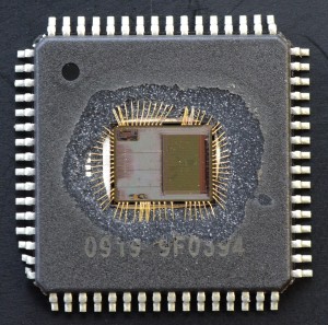
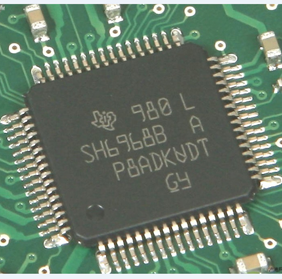
16 years deep in the reverse analysis of integrated circuit technology, senior technical team, skilled, experienced in a variety of blind buried hole PCB , laser blind hole board, UHF board, ceramic board , component density, all over the microstrip lines and other long lines, high-frequency processing requirements and strict control of electromagnetic compatibility of the communication board copy
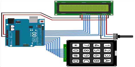
Recent Project
Recent Project
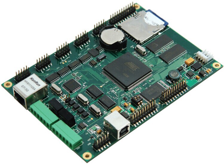
Recent Project
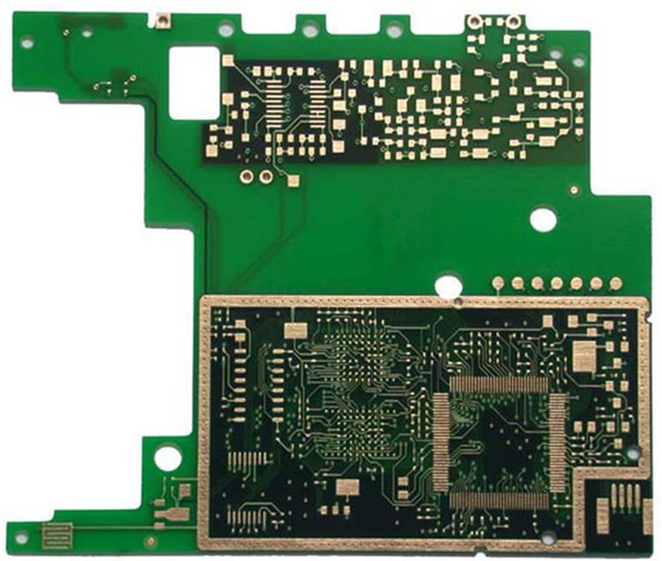
Recent Project
All about PCB Reverse Engineering & IC Crack

Introduction to Crosstalk in High-speed PCB Design In today’s world of high-speed electronic systems, printed circuit board (PCB) designs are becoming increasingly complex. A
Introduction to PCB Current Calculator A PCB (Printed Circuit Board) Current Calculator is an essential tool for electronics engineers and hobbyists who design and work with PCBs.
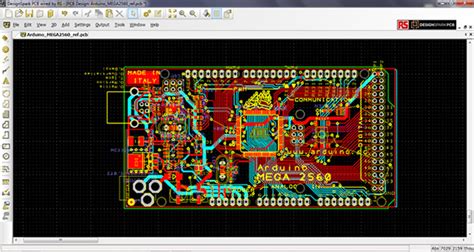
Introduction to DesignSpark PCB DesignSpark PCB is a powerful, easy-to-use printed circuit board (PCB) design software for Windows PCs. Developed by RS Components, DesignSpark PCB