Analysis and Control of crosstalk in high speed PCB design
Introduction to Crosstalk in High-speed PCB Design In today’s world of high-speed electronic systems, printed circuit board (PCB) designs are becoming increasingly complex. A
PCB REVERSE ENGINEERING
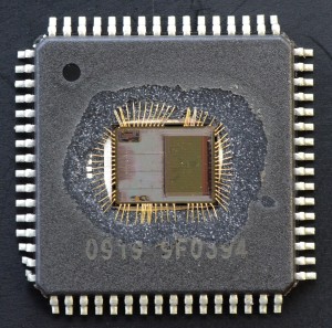
IC Unlock + PCB Reverse engineering Services - We will crack your IC sample. You will receive IC program in Bin / Hex file for burning any new ICs
PCB to schematic, Schematic to Gerber file, PCBA to Schematic Gerber & Bom List
We focus on a strategy of continuous customer-centric innovation. The goal is to deliver timely solutions for anticipated and actual customer.
We offer our customers from around the world to maintain a very good communication and product support services.
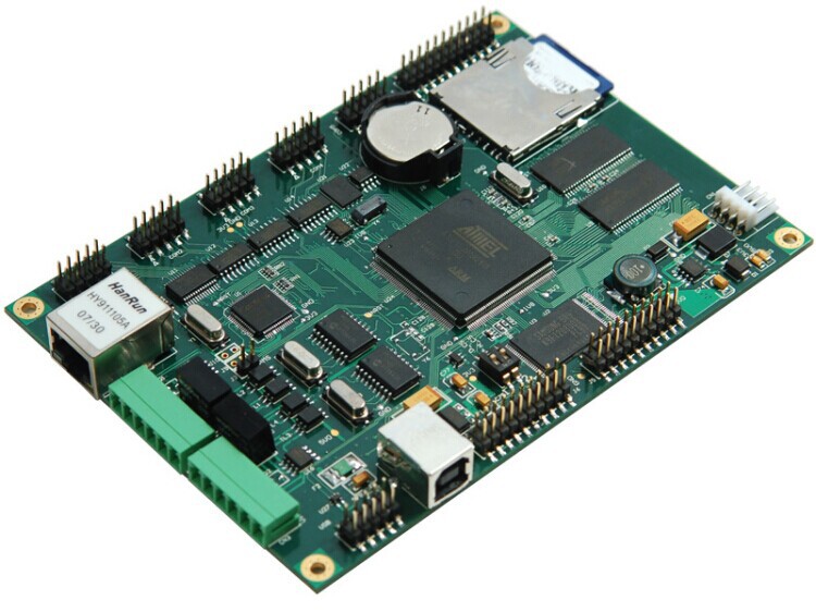
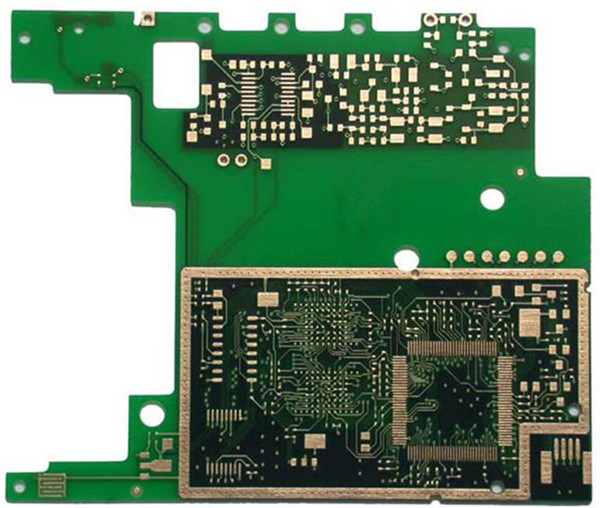
We will reverse engineer your PCB sample, and deilver the engineering file into:1. PCB 2. Gerber File 3. BOM List 4. Schematic Diagram
16 years deep in the reverse analysis of integrated circuit technology, senior technical team, skilled, experienced in a variety of blind buried hole PCB , laser blind hole board, UHF board, ceramic board , component density, all over the microstrip lines and other long lines, high-frequency processing requirements and strict control of electromagnetic compatibility of the communication board copy


All about PCB Reverse Engineering & IC Crack
Introduction to Crosstalk in High-speed PCB Design In today’s world of high-speed electronic systems, printed circuit board (PCB) designs are becoming increasingly complex. A
Introduction to PCB Current Calculator A PCB (Printed Circuit Board) Current Calculator is an essential tool for electronics engineers and hobbyists who design and work with PCBs.
Introduction to DesignSpark PCB DesignSpark PCB is a powerful, easy-to-use printed circuit board (PCB) design software for Windows PCs. Developed by RS Components, DesignSpark PCB