DS1307 Pinout: An in-depth Guide to the Real-Time Clock IC
Introduction to the DS1307 Real-Time Clock The DS1307 is a popular real-time clock (RTC) integrated circuit used in many electronic projects and products to keep accurate time. It
16 years deep in the reverse analysis of integrated circuit technology, senior technical team, skilled, experienced in a variety of blind buried hole PCB , laser blind hole board, UHF board, ceramic board , component density, all over the microstrip lines and other long lines, high-frequency processing requirements and strict control of electromagnetic compatibility of the communication board copy
Recent Project
Recent Project
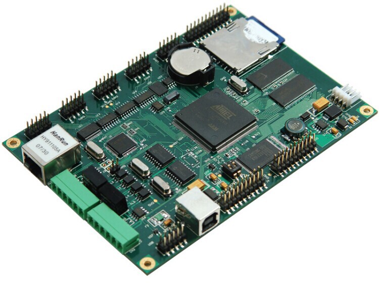
Recent Project
Recent Project
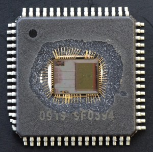
All about PCB Reverse Engineering & IC Crack
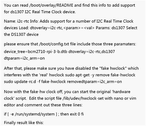
Introduction to the DS1307 Real-Time Clock The DS1307 is a popular real-time clock (RTC) integrated circuit used in many electronic projects and products to keep accurate time. It
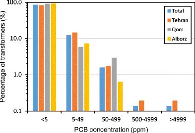
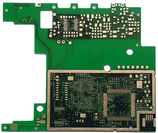
Introduction to PCB Contamination Printed Circuit Boards (PCBs) are the backbone of modern electronic devices. They are used in a wide range of applications, from consumer electron
Key Features of the MMBT3904 Transistor The MMBT3904 transistor offers several key features that make it a popular choice for various electronic circuits: High Switching Speed: T