PCB Assembly Process-9 Tips On How To Ensure a Smooth PCB Assembly Process
The PCB Assembly Process: An Overview Before diving into the tips, let’s review the main steps of the PCB assembly process at a high level: Design & Manufacturing: It a
16 years deep in the reverse analysis of integrated circuit technology, senior technical team, skilled, experienced in a variety of blind buried hole PCB , laser blind hole board, UHF board, ceramic board , component density, all over the microstrip lines and other long lines, high-frequency processing requirements and strict control of electromagnetic compatibility of the communication board copy
Recent Project
Recent Project
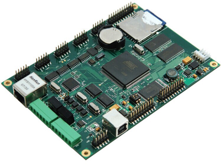
Recent Project
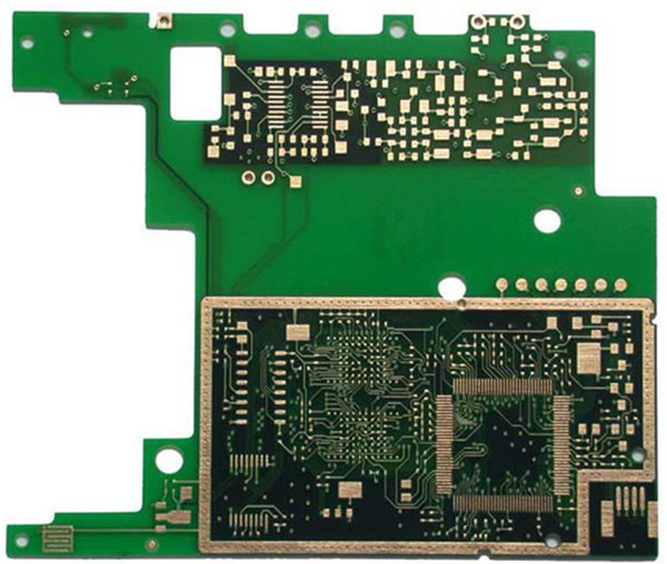
Recent Project
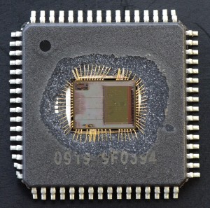
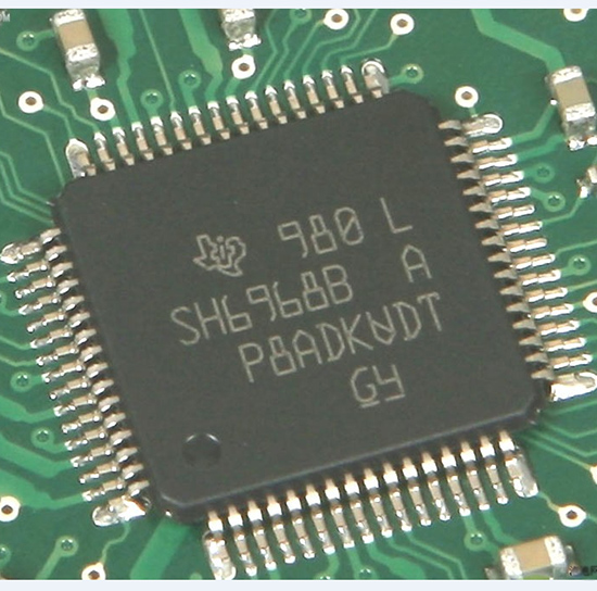
All about PCB Reverse Engineering & IC Crack
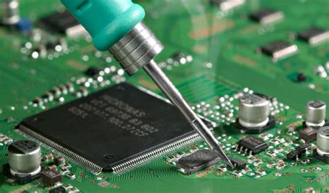
The PCB Assembly Process: An Overview Before diving into the tips, let’s review the main steps of the PCB assembly process at a high level: Design & Manufacturing: It a

The Insatiable Acquisition Appetite of Maxim Integrated Maxim Integrated Products, Inc., a leading global manufacturer of analog and mixed-signal integrated circuits, has a long hi
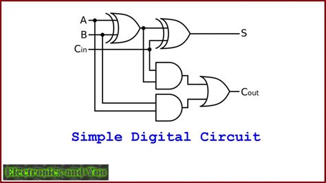
Introduction to Electro Schematics Electro schematics, also known as circuit diagrams or electrical schematics, are visual representations of electrical circuits. They use standard