PCB Manufacturers-Introducing Valuable From China
Introduction to PCB Manufacturing in China China has emerged as a global leader in the manufacturing of Printed Circuit Boards (PCBs). The country's PCB industry has experienced tr
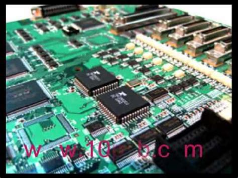
16 years deep in the reverse analysis of integrated circuit technology, senior technical team, skilled, experienced in a variety of blind buried hole PCB , laser blind hole board, UHF board, ceramic board , component density, all over the microstrip lines and other long lines, high-frequency processing requirements and strict control of electromagnetic compatibility of the communication board copy
Recent Project
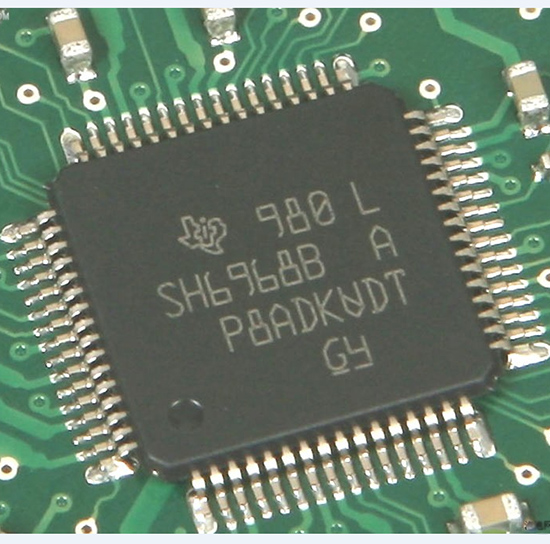
Recent Project
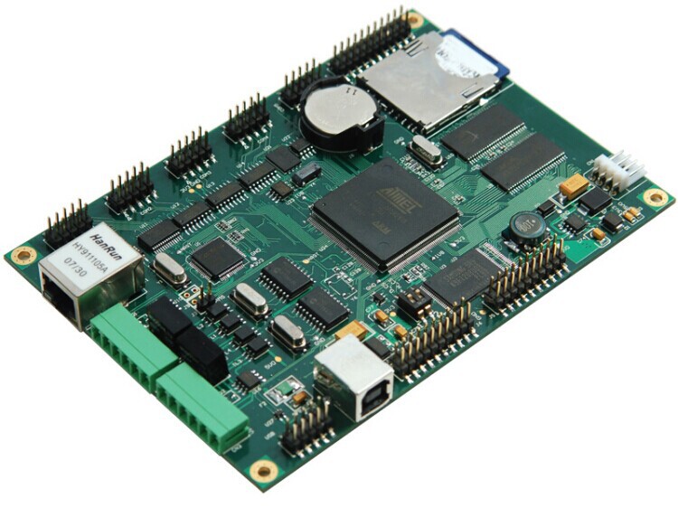
Recent Project
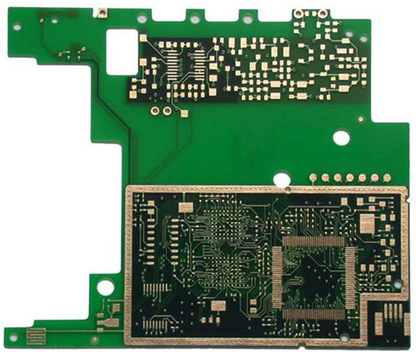
Recent Project
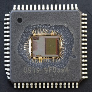
All about PCB Reverse Engineering & IC Crack
Introduction to PCB Manufacturing in China China has emerged as a global leader in the manufacturing of Printed Circuit Boards (PCBs). The country's PCB industry has experienced tr
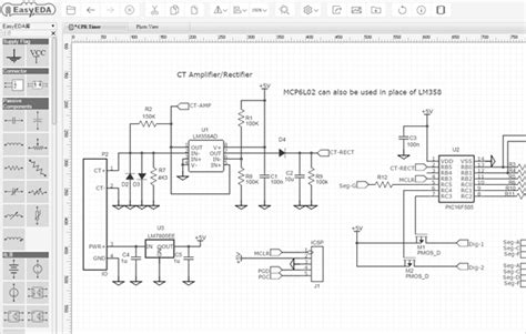
What are Circuit Simulators? Circuit simulators are software tools that allow you to create and simulate electronic circuits on a computer. They provide a virtual environment where
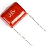
Introduction to X-Rated Capacitors X-rated capacitors, also known as across-the-line capacitors or line-to-line capacitors, are essential components in transformerless power suppli