PCB Prototype: What Is It and Why You Need One
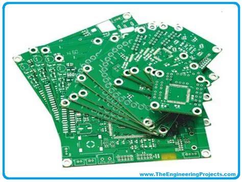
What is a PCB Prototype? A PCB (Printed Circuit Board) prototype is a preliminary version of a printed circuit board that is used for testing and validation before mass production.
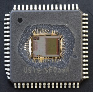
16 years deep in the reverse analysis of integrated circuit technology, senior technical team, skilled, experienced in a variety of blind buried hole PCB , laser blind hole board, UHF board, ceramic board , component density, all over the microstrip lines and other long lines, high-frequency processing requirements and strict control of electromagnetic compatibility of the communication board copy
Recent Project
Recent Project
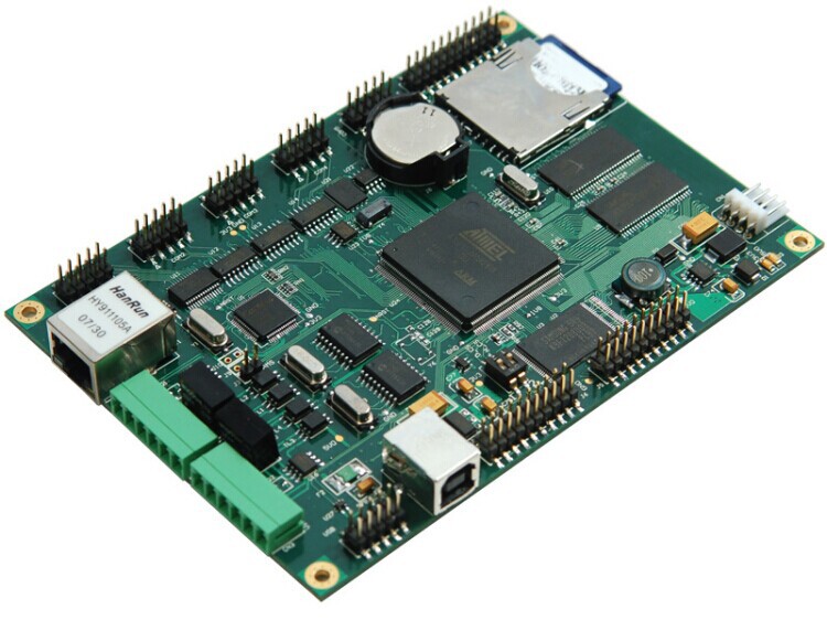
Recent Project
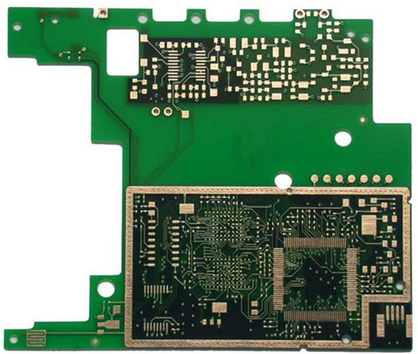
Recent Project
All about PCB Reverse Engineering & IC Crack
What is a PCB Prototype? A PCB (Printed Circuit Board) prototype is a preliminary version of a printed circuit board that is used for testing and validation before mass production.
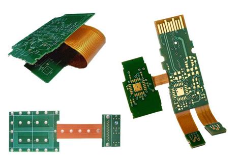
Introduction to Flexible PCBs Flexible Printed Circuit Boards (FPCBs) have gained immense popularity in recent years due to their unique characteristics and versatile applications.
What is a PCB Turnkey Service? A PCB (Printed Circuit Board) turnkey service is a comprehensive solution provided by electronics manufacturing companies that encompasses the entire