
What is AutoCAD?
AutoCAD is a versatile computer-aided design (CAD) software developed by Autodesk. It is widely used across various industries for creating precise 2D and 3D designs. AutoCAD offers a comprehensive set of tools and features that enable users to create, modify, and document their designs efficiently.
Can AutoCAD be used for PCB design?
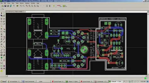
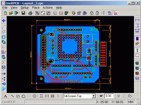
While AutoCAD is not specifically designed for printed circuit board (PCB) design, it can be used for this purpose with some limitations. AutoCAD lacks some of the specialized features and libraries found in dedicated PCB design software. However, it can still be a useful tool for creating basic PCB layouts and schematic diagrams.
Advantages of using AutoCAD for PCB design
- Familiarity: Many engineers and designers are already proficient in using AutoCAD, which can make the transition to PCB design easier.
- Versatility: AutoCAD’s wide range of tools and features can be adapted for PCB design tasks.
- Integration: AutoCAD files can be easily shared and integrated with other software used in the PCB design process.
Limitations of using AutoCAD for PCB design
- Lack of specialized tools: AutoCAD does not have built-in tools for tasks such as component placement, trace routing, and design rule checks (DRC).
- Limited libraries: AutoCAD does not come with extensive libraries of PCB components and footprints, which can slow down the design process.
- No simulation capabilities: AutoCAD does not have integrated simulation tools for analyzing signal integrity, power delivery, or electromagnetic compatibility.
Setting up AutoCAD for PCB design
Creating a custom workspace
To optimize AutoCAD for PCB design, you can create a custom workspace with frequently used tools and commands. Here’s how:
- Open AutoCAD and click on the “Workspace Switching” icon in the bottom-right corner of the screen.
- Select “Manage Workspaces” from the dropdown menu.
- In the “Workspace Manager” dialog box, click “New.”
- Enter a name for your custom workspace, such as “PCB Design,” and click “OK.”
- Customize the ribbon, toolbars, and palettes to include the tools and commands you need for PCB design.
- Click “OK” to save your custom workspace.
Setting up layers and line types
Organizing your PCB design into layers and using appropriate line types can help keep your drawing clean and easy to read. Here’s a suggested layer setup:
| Layer Name | Color | Line Type | Description |
|---|---|---|---|
| Board Outline | Blue | Continuous | PCB outline and dimensions |
| Top Copper | Red | Continuous | Top layer copper traces |
| Bottom Copper | Green | Continuous | Bottom layer copper traces |
| Top Silkscreen | Magenta | Continuous | Top layer silkscreen graphics and text |
| Bottom Silkscreen | Cyan | Continuous | Bottom layer silkscreen graphics and text |
| Top Solder Mask | Brown | Continuous | Top layer solder mask openings |
| Bottom Solder Mask | Purple | Continuous | Bottom layer solder mask openings |
| Drills | White | Continuous | Drill holes and vias |
| Notes | Yellow | Continuous | Design notes and annotations |
To create these layers and assign line types:
- Open the “Layer Properties Manager” by typing “LAYER” in the command line and pressing Enter.
- Click the “New Layer” icon to create each layer, assigning the appropriate name, color, and line type.
- Click “OK” to close the “Layer Properties Manager.”

Creating a PCB layout in AutoCAD
Drawing the board outline
Start by drawing the outline of your PCB using the “POLYGON” or “RECTANGLE” command. Place this outline on the “Board Outline” layer.
Placing components
- Create a block for each component in your design using the “BLOCK” command. Include the component footprint and any necessary pin designations.
- Insert instances of these component blocks onto your PCB layout using the “INSERT” command.
- Position the components as desired, ensuring proper spacing and orientation.
Routing traces
- Use the “POLYLINE” command to draw traces between component pins on the “Top Copper” and “Bottom Copper” layers.
- Ensure that your traces meet the minimum width and spacing requirements for your PCB manufacturer and design rules.
- Use the “OFFSET” command to create parallel traces when necessary.
Adding vias and drills
- Use the “CIRCLE” command to place vias and drill holes on the “Drills” layer.
- Ensure that your vias and drills meet the minimum size and spacing requirements for your PCB manufacturer.
Creating silkscreen graphics and text
- Use the “TEXT” and “MTEXT” commands to add text annotations, such as component designators and pin numbers, on the “Top Silkscreen” and “Bottom Silkscreen” layers.
- Use the “POLYLINE” and other drawing commands to create graphic elements, such as logos or assembly instructions, on the silkscreen layers.
Adding solder mask openings
- Use the “OFFSET” command to create solder mask openings around pads and vias on the “Top Solder Mask” and “Bottom Solder Mask” layers.
- Ensure that your solder mask openings meet the minimum size and spacing requirements for your PCB manufacturer.
Exporting your PCB design
Generating Gerber files
Gerber files are the industry standard format for PCB manufacturing. To generate Gerber files from your AutoCAD PCB design:
- Open the “Plot” dialog box by typing “PLOT” in the command line and pressing Enter.
- Select the “Gerber” device from the “Printer/plotter” dropdown menu.
- Choose the appropriate settings for your Gerber files, such as format (e.g., RS-274X), units, and aperture size.
- Select the layers you want to export, such as copper, silkscreen, and solder mask layers.
- Click “OK” to generate the Gerber files.
Generating drill files
Drill files contain information about the location and size of drills and vias in your PCB design. To generate drill files:
- Open the “Plot” dialog box by typing “PLOT” in the command line and pressing Enter.
- Select the “NC Drill” device from the “Printer/plotter” dropdown menu.
- Choose the appropriate settings for your drill files, such as format (e.g., Excellon), units, and hole size.
- Select the “Drills” layer to export.
- Click “OK” to generate the drill files.
Conclusion
While AutoCAD may not be the ideal choice for complex PCB designs, it can be used for basic PCB layout and schematic creation. By setting up a custom workspace, organizing layers, and following best practices for component placement and trace routing, you can create functional PCB designs in AutoCAD. However, for more advanced PCB design tasks, it is recommended to use dedicated PCB design software with specialized tools and libraries.
FAQ
1. Can I use AutoCAD for multi-layer PCB designs?
Yes, you can create multi-layer PCB designs in AutoCAD by assigning different layers to represent each copper layer, such as “Top Copper,” “Bottom Copper,” and “Inner Layer 1.” However, managing multi-layer designs in AutoCAD can be more challenging than in dedicated PCB design software.
2. Are there any AutoCAD plugins or libraries for PCB design?
There are some third-party plugins and libraries available that can extend AutoCAD’s capabilities for PCB design. For example, the “PCB Library Wizard” is a free plugin that allows you to create and manage PCB footprints and components in AutoCAD. However, these plugins may not be as comprehensive as the tools found in dedicated PCB design software.
3. Can I import AutoCAD PCB designs into other PCB design software?
Yes, most dedicated PCB design software can import AutoCAD DWG or DXF files. However, you may need to make some adjustments to the imported design to ensure compatibility with the PCB software’s tools and features.
4. How do I check for design rule violations in AutoCAD?
AutoCAD does not have built-in design rule check (DRC) tools for PCB design. To check for design rule violations, you will need to manually inspect your design or use third-party plugins that offer DRC functionality. Alternatively, you can export your design to a dedicated PCB design software and perform DRC there.
5. Can I create a bill of materials (BOM) for my PCB design in AutoCAD?
AutoCAD does not have built-in tools for generating a bill of materials (BOM) for PCB designs. However, you can manually create a BOM by listing the components used in your design in a separate document or spreadsheet. Some third-party plugins may also offer BOM generation capabilities for AutoCAD PCB designs.