Magnetic resonance PCB secondary development for medical devices
Medical device MRI Control PCB Copy
Imaging Principle
A medical magnetic resonance imaging system (MRI) consists of a magnet, a coil, a control unit, a computer imaging system and a diagnostic bed. MRI is a biomagnetic nuclear spin imaging technology that has been rapidly developed with the development of computer technology, electronic circuit technology, and superconductor technology. It uses magnetic field and radio frequency pulses to make the hydrogen nucleus (H+) in human tissue in spin motion vibrate to produce radio frequency signals, which are imaged by computer processing. That is, there is a stable magnetic field and an alternating electromagnetic field acting on the sample. After removing the electromagnetic field, the nucleus in the excited state can jump to a lower energy level and radiate electromagnetic waves, and at the same time, a voltage signal can be induced in the coil, which becomes the nuclear magnetic resonance signal. Human tissues contain a large number of hydrogen nuclei due to the presence of large amounts of water and hydrocarbons, and the signals obtained with hydrogen nuclei are generally more than 1000 times larger than other nuclei. The water in human body organs and tissues is not the same, and the pathological process of many diseases will lead to the change of water morphology, which makes the voltage signal of normal tissues different from that of diseased tissues. Combined with the electronic computed tomography (CT) technology, we can get the image of any section of human tissues, especially for the diagnosis of soft tissue lesions, which shows its advantages, the lesion area is very sensitive and the image is clear. If the number of frequency variables of MRI is increased to two or more, two-dimensional or multi-dimensional MRI can be achieved, thus obtaining more information than one-dimensional MRI.
Magnetic field intensity meter: The resolving power is 0.1mT, and the maximum allowable error is not more than one-third of the object to be examined.
The test was performed according to the method recommended by AAPM and the method in the module manual. The performance parameters tested were signal-to-noise ratio, uniformity, linearity error (aberration), layer thickness error, spatial resolving power and low contrast resolving power. Firstly, the performance parameters were grouped according to the field strength, and the relationship between the performance parameters and the field strength was studied. Then, the uniformity, linearity error (aberration), layer thickness error, spatial resolution and low contrast resolution were grouped according to their sizes, and the distribution characteristics of the performance parameters were studied.
3.2.1 Signal-to-noise ratio
All the equipment is divided into 4 groups according to the field strength, the first group field strength <0.5T, for low field strength; the second group field strength of 0.5T ~ 0.9T; the third group field strength of 1.0T ~ 1.5T; the fourth group field strength ≥ 1.5T. Table 2 shows the maximum value, minimum value, extreme difference and average value of signal-to-noise ratio under 4 groups field strength. The average value of S/N ratio varies greatly from group to group, and increases obviously with the increase of field strength.
3.2.2 Uniformity
Uniformity is grouped by field strength, and there is no significant difference in uniformity among groups, see Table 3.
Equipment if grouped by uniformity, the number and percentage of units in each group is shown in Table 4. 97.5% or more of the equipment uniformity in more than 94%, 100% of the equipment uniformity in more than 90%.
3.2.3 Linearity error (aberration)
X-direction linearity error (aberration) grouped by field strength, the average value of X-direction linearity error of each group does not differ significantly, see Table 5.
Equipment if the X-direction linearity error (aberration) grouping, the number and percentage of each group as shown in Table 6. 97.5% or more of the equipment X-direction linearity error (aberration) in less than 5%, 2.5% of the equipment X-direction linearity error (aberration) more than 5%.
Y-direction linearity error (aberration) by field strength grouping, the average value of the Y-direction linearity error of each group is not significantly different, see Table 7. if the linearity error by Y-direction grouping, the number of units in each group and the percentage of Table 8. 97.5% or more of the equipment Y-direction linearity error (aberration) in 1.5% or less, 100% of the equipment Y-direction linearity error (aberration) in 3.5% or less.
3.2.4 Layer thickness error
The layer thickness of 8 devices could not be measured because the signal of some devices’ slant line image was too weak and some devices had no Profile function. For the 32 devices that have measured the layer thickness grouped by field strength, there is no significant difference in the layer thickness error of each group, see Table 9.
If grouped by the size of the layer thickness error, the number of units in each group and the percentage of Table 10. 90% of the equipment layer thickness error is less than 1.0mm, 10% of the equipment layer thickness error is more than 1mm.
3.2.5 Spatial resolution
Because the highest spatial resolution of the device is equal to the size of the pixel, in the measurement of spatial resolution FOV is taken as 256mm, pixel matrix is taken as 256×256, pixel is equal to 1mm, so the highest spatial resolution of the device is equal to 1mm. according to the results of field strength grouping, there is no significant difference in the spatial resolution of each group, see Table 11.
Among the 40 devices, 80% of the devices with spatial resolution of 1mm and 20% of the devices with spatial resolution of 1.25mm.
3.2.6 Low-contrast resolving power
According to the field strength grouping, the low contrast resolution is related to the field strength, as shown in Table 12. the devices with the field strength equal to and higher than 0.5T can distinguish the hole of Φ4mm/0.5mm deep, among the devices with the field strength lower than 0.5T, the devices with the low contrast resolution of Φ4mm/0.5mm deep account for 83%, and the devices with Φ6mm/0.5mm deep account for 17%
4 Discussion
The criteria for MRI clinical application performance proposed in the AAPM 100 report are quality assurance standards that are applicable to all manufacturers and models of equipment. Based on the statistical analysis of the test results of 40 MRI devices of different manufacturers and different field strengths, the following evaluations of the relevant standards were made:
4.1 Signal-to-noise ratio with respect to field strength
The field strengths of the 40 MRI devices were divided into the following four groups: <0.5 T, 0.5 T to 0.9 T, 1.0 T to 1.5, and ≥1.5 T. The average signal-to-noise ratio of each group increased with field strength, and was 77, 112, 194, and 270, respectively. The AAPM report did not propose a standard for signal-to-noise ratio, and different standards must be adopted for different field strengths if a standard for signal-to-noise ratio is to be specified.
4.2 Uniformity is independent of field strength
Among the 40 MRI devices, 100% of the devices had a uniformity of 90% or more. the uniformity standard recommended by the AAPM report is 80%, which is too low from the results of the experimental tests. With the advancement of MRI technology and the improvement of equipment performance, this performance has generally improved.
4.3 Linearity errors (aberrations) are independent of field strength
The linearity error recommended by the AAPM report is 5%, and the results of the test show that this standard is appropriate.
4.4 Layer thickness error is independent of field strength
Among the 32 devices with measured layer thickness, 90% of the devices have layer thickness error less than 1.0mm, and 10% of the devices have layer thickness error more than 1.0mm. The standard of layer thickness error introduced by the AAPM report is ±1mm, and the standard is also appropriate from the test results.
4.5 Spatial resolution is independent of field strength
The spatial resolution standard introduced by the AAPM report is 1mm, which is the ideal spatial resolution, from the test results only 79.4% of the equipment can reach this standard, there are still 20.6% of the equipment can not reach. The standard as a quality assurance standard is okay, but as the standard of clinical application quality is too high, according to the standard, there will be part of the equipment clinical application quality failed.
4.6 Low-contrast resolving power related to field strength
This parameter is not included in the performance parameters of MRI equipment proposed in the AAPM report, but we believe that this parameter is indispensable. Because the low contrast resolution is different from the spatial resolution, the latter is the ability to distinguish the target under high contrast conditions, and the former is the ability to distinguish the target under low contrast conditions, both are performance parameters directly related to the quality of clinical diagnosis. The low-contrast resolution can be quantitatively detected by specially designed body model. From the results of experimental testing, the low-contrast resolution is related to the field strength, and the devices with the field strength equal to or higher than 0.5T can distinguish the holes of Φ4mm/0.5mm deep, and 83% of the devices with the field strength lower than 0.5T can distinguish the holes of Φ4mm/0.5mm deep, and 17% of the devices can distinguish the holes of Φ6mm/0.5mm deep. 0.5mm deep hole. Therefore, the low contrast resolution standard should be set according to the different field strength.
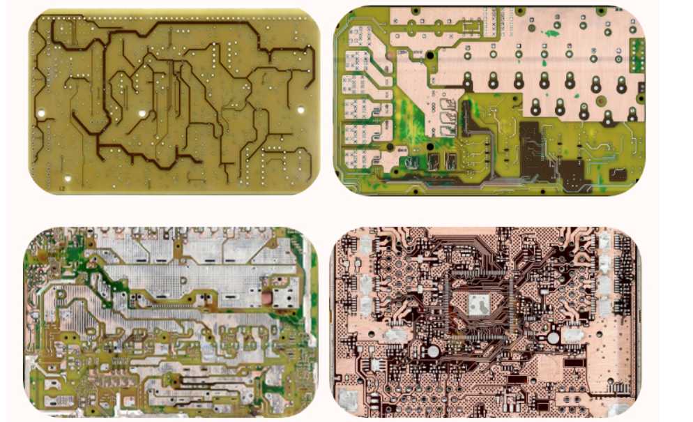
Our PCB copy board team has accumulated 17 years of technical experience in Shenzhen and has been involved in almost all electronic products PCB circuit boards, especially for various high-precision special circuit boards and various multi-layer PCB copy board experience for many years, and has a better understanding of the structure and alignment rules of complex PCB boards containing laser holes, blind holes and buried holes. Under the premise of the reverse R & D technology means to reverse analysis of the circuit board, the original product PCB files, bill of materials (BOM) files, schematic files and other technical documents and PCB screen printing production files for 1:1 restoration, and then use these technical documents and production files for PCB board, component welding, flying probe test, circuit board debugging, complete the original circuit board prototype board complete copy of the original circuit board prototype.
With the advanced scanning technology, the latest copy software and the most experienced senior technical team in China, we have been providing various single-layer, double-layer, multi-layer PCB board copy, various blind buried hole boards, laser blind hole boards, UHF boards, ceramic PCB copy boards, component density, long lines all over the microstrip lines, high frequency processing requirements and strict EMC control of the communication board copy services, customers only need to provide a complete set of sample boards or a complete set of sample boards. Customers only need to provide a complete set of prototypes or prototypes, Qingbao Technology promises to copy the board at once, change the board, debugging, copy the accuracy of the board to 1mil.