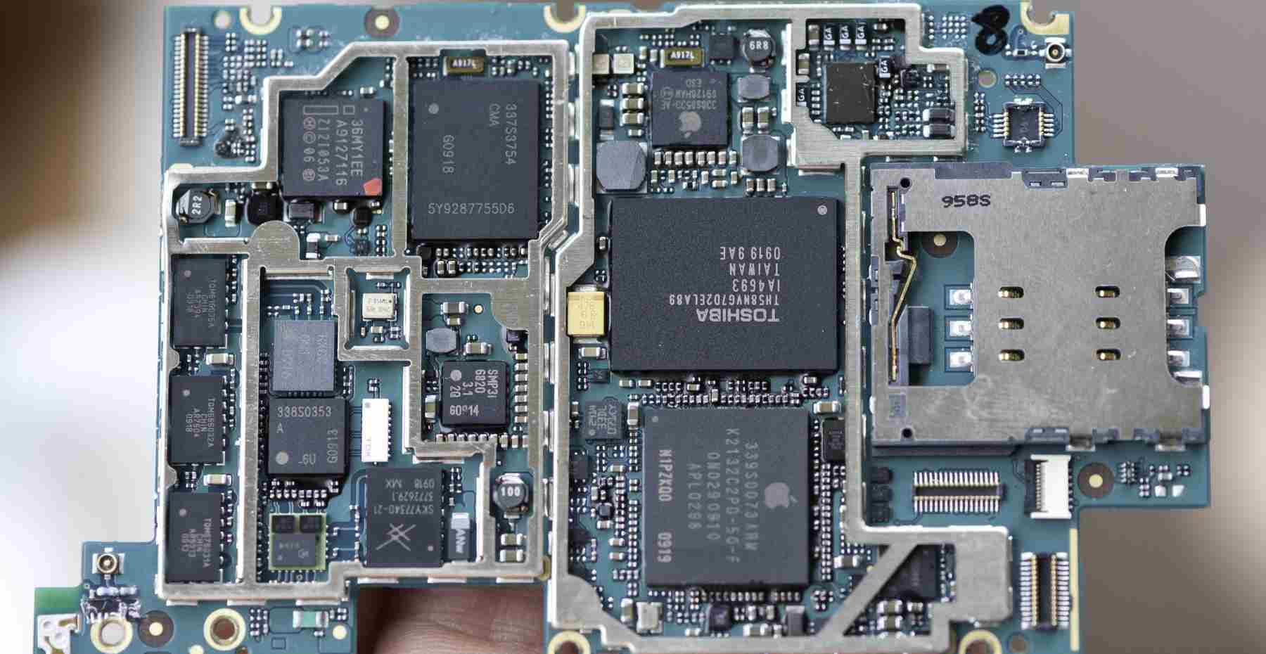
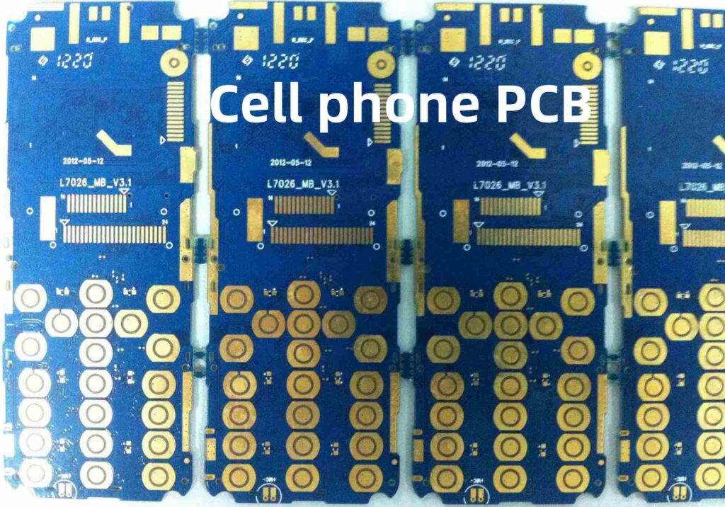
Cell phone PCB copy board, cell phone board with many functions and components, but the PCB space is small, cell phone board PCB copy board rewriting of the wiring design of the restoration to go to the highest. Usually need four to six layers of PCB board. High-power circuits include RF buffers and voltage-controlled oscillators (VCO). Make sure that the PCB board on the high power area at least a block of land, preferably without over-hole above, the more copper skin the better. Sensitive analog signals should be as far away as possible from high-speed digital signals and RF signals.2. Design partitioning can be broken down into physical and electrical partitioning.
Physical partitioning mainly involves component layout, orientation and shielding; electrical partitioning can continue to be broken down into partitions for power distribution, RF alignment, sensitive circuits and signals, and grounding.
Physical Partitioning
Component layout is the key to achieving a good RF design, and the most effective technique is to first fix the components located in the RF path and adjust their orientation to minimize the length of the RF path, keeping the inputs away from the outputs and separating high power circuits from low power circuits as far as possible.
The most efficient stacking method is to arrange the main ground plane (main ground) on the second layer under the surface layer and route the RF lines on the surface layer whenever possible. Minimizing the size of the vias in the RF path not only reduces path inductance, but also reduces false solder points on the main ground and reduces the chance of RF energy leakage to other areas within the laminate.
In physical space, linear circuits like multi-stage amplifiers are usually sufficient to isolate multiple RF zones from each other, but duplexers, mixers, and IF amplifiers/mixers always have multiple RF/IF signals interfering with each other, so this effect must be carefully minimized.
RF and IF alignment
RF and IF alignment should be crossed as far as possible, and as far as possible in between them separated by a piece of ground.
The correct RF path is very important to the performance of the entire PCB board, which is why component layout usually takes up most of the time in the design of cell phone PCBs.
On the cell phone PCB board design, you can usually put the low noise amplifier circuit on one side of the PCB board, and the high power amplifier on the other side, and eventually connect them to the RF side and the baseband processor side of the antenna on the same side through the duplexer. Some skill is needed to ensure that the straight-through holes do not transfer RF energy from one side of the board to the other side, and a common technique is to use blind holes on both sides. The adverse effects of straight-through holes can be minimized by arranging them in areas where both sides of the PCB are free from RF interference. Sometimes it is not possible to ensure sufficient isolation between multiple circuit blocks, in this case it is necessary to consider the use of metal shields to shield RF energy in the RF region, metal shields must be soldered to the ground, must be maintained at an appropriate distance from the components, and therefore need to take up valuable PCB board space. It is very important to ensure the integrity of the shield as much as possible, the digital signal lines into the metal shield should go as far as possible to the inner layer, and it is best to go to the line layer of the PCB is a layer below the ground layer.
RF signal lines can go from the metal shield at the bottom of the small gap and ground gap in the wiring layer, but the gap around as much as possible to lay some ground, different layers on the ground can be connected together through multiple vias.
Decoupling circuit
Many RF chips with integrated linear lines are very sensitive to power supply noise, and usually each chip requires up to four capacitors and an isolation inductor to ensure that all power supply noise is filtered out. An integrated circuit or amplifier often with an open-drain output, so a pull-up inductor is required to provide a high-impedance RF load and a low-impedance DC power supply, the same principle applies to the power supply at the end of this inductor to decouple.
Some chips require multiple power supplies to operate, so you may need two or three sets of capacitors and inductors to decouple them separately. Inductors are rarely placed in parallel, as this creates a null-core transformer and induces interference signals, so they should be at least as far apart as the height of one of the devices, or arranged at right angles to minimize their mutual inductance.
Electrical partitioning
Some parts of the phone use different operating voltages and control them with the help of software to extend the battery operating life. This means that the phone needs to run multiple power supplies, and this poses additional problems for isolation.
Power is usually brought in from a connector and immediately decoupled to filter out any noise from outside the board, then distributed after a set of switches or regulators.
The DC current of most circuits on a cell phone PCB is quite small, so the alignment width is usually not an issue, however, a separate high current line as wide as possible must be run for the power supply of the high power amplifier to minimize the transmission voltage drop.
To avoid too much current loss, multiple vias are required to pass current from one layer to another. In addition, if the power supply pins of the high power amplifier cannot be sufficiently decoupled at its end, then high power noise will radiate throughout the board and cause a variety of problems.
The grounding of high power amplifiers is quite critical and often requires a metal shield to be designed for them. In most cases, it is also critical to ensure that the RF output is kept away from the RF input. This also applies to amplifiers, buffers and filters in the best case scenario, they will be able to operate stably at any temperature and voltage conditions. In reality, they can become unstable and add noise and intermodulation signals to the RF signal. If the RF signal line has to be wound from the input of the filter back to the output, this can seriously damage the bandpass characteristics of the filter.
In order to get good isolation of the input and output, first a ground must be laid around the filter, and secondly a ground should be laid in the lower area of the filter and connected to the main ground surrounding the filter. It is also a good idea to place the signal lines that need to pass through the filter as far away from the filter pins as possible.
In addition, the entire board should be grounded very carefully in various places, otherwise a coupling channel will be introduced. Sometimes you can choose to go single-ended or balanced RF signal lines, the principles of cross-talk and EMC/EMI also apply here. Balanced RF signal lines can reduce noise and cross-talk if routed correctly, but their impedance is usually higher, and to maintain a reasonable line width to get a matching signal source, alignment and load impedance, the actual wiring may have some difficulties.