How to solve the problem of QFP solder bridging
What is QFP solder bridging?
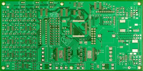
QFP (Quad Flat Package) is a surface-mount integrated circuit package with leads extending from each of the four sides. QFP packages are commonly used for microcontrollers, microprocessors, and other complex ICs.
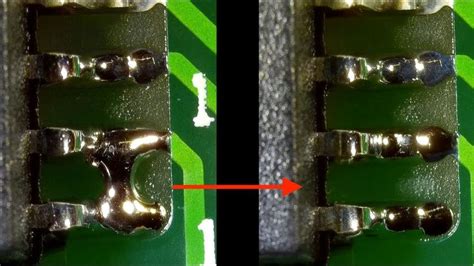
Solder bridging is a defect that occurs when solder inadvertently connects adjacent pins or pads, creating an unintended short circuit. QFP packages are particularly prone to solder bridging due to the fine pitch (small spacing) between the leads.
Solder bridging can cause various issues, such as:
– Malfunctioning or non-functioning devices
– Intermittent problems that are difficult to diagnose
– Reduced reliability and product lifespan
– Increased manufacturing costs due to rework or scrap
Causes of QFP Solder Bridging
Several factors can contribute to the occurrence of solder bridging in QFP packages:
1. Inadequate Solder Paste Printing
Inconsistent or excessive solder paste application can lead to solder bridging. This can be caused by:
– Worn or damaged stencils
– Improper stencil thickness
– Incorrect stencil aperture size or shape
– Poor stencil alignment
– Inadequate stencil cleaning
2. Improper Reflow Profile
An incorrect reflow profile can cause solder bridging by:
– Insufficient preheating, leading to cold solder joints
– Excessive peak temperature, causing solder splatter
– Inadequate cooling rate, allowing solder to flow between leads
3. Component Placement Issues
Inaccurate component placement can result in solder bridging, especially if the leads are not properly aligned with the pads. Common causes include:
– Poor pick-and-place machine calibration
– Incorrect component orientation
– Bent or misaligned leads
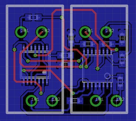
4. PCB Design Flaws
PCB design issues can contribute to solder bridging, such as:
– Insufficient pad-to-pad spacing
– Inadequate solder mask clearance
– Incorrect pad size or shape
5. Environmental Factors
Environmental conditions can also impact solder bridging, including:
– High humidity, which can cause solder paste slumping
– Dust or debris contamination
– Electrostatic discharge (ESD) events

Preventing QFP Solder Bridging
To minimize the occurrence of QFP solder bridging, consider the following preventive measures:
1. Optimize Solder Paste Printing
Ensure consistent and accurate solder paste application by:
– Using high-quality, well-maintained stencils
– Selecting the appropriate stencil thickness and aperture size
– Implementing proper stencil alignment and cleaning procedures
– Regularly inspecting and replacing worn or damaged stencils
2. Fine-tune Reflow Profile
Develop and optimize the reflow profile for each specific PCB Assembly by:
– Conducting thermal profiling to ensure proper preheating, peak temperature, and cooling rates
– Adjusting the reflow profile based on the solder paste manufacturer’s recommendations
– Monitoring and controlling oven temperature and conveyor speed
3. Improve Component Placement Accuracy
Ensure precise component placement by:
– Regularly calibrating and maintaining pick-and-place machines
– Using vision systems to verify component orientation and alignment
– Inspecting components for bent or misaligned leads prior to placement
4. Optimize PCB Design
Design PCBs with solder bridging prevention in mind by:
– Providing adequate pad-to-pad spacing, especially for fine-pitch QFP packages
– Ensuring proper solder mask clearance around pads
– Optimizing pad size and shape for improved solder joint formation
5. Control Environmental Conditions
Maintain a clean and controlled manufacturing environment by:
– Regulating humidity levels to prevent solder paste slumping
– Implementing strict cleanliness protocols to minimize dust and debris
– Utilizing ESD Protection measures to prevent electrostatic discharge events

Detecting and Reworking QFP Solder Bridges
Despite preventive measures, solder bridging may still occur. Early detection and proper rework techniques are crucial for minimizing the impact on product quality and manufacturing costs.
1. Visual Inspection
Visual inspection is the most common method for detecting solder bridges. This can be done using:
– Magnifying lenses or microscopes
– Automated optical inspection (AOI) systems
– X-ray inspection for hidden solder bridges
When visually inspecting QFP packages for solder bridges, pay close attention to:
– Adjacent leads or pads that appear to be connected by solder
– Solder that extends beyond the pad edges
– Irregular or excessive solder joint shapes
2. Electrical Testing
Electrical testing can help identify solder bridges that may not be visible during visual inspection. Common electrical testing methods include:
– In-circuit testing (ICT)
– Flying Probe testing
– Boundary scan testing
These methods can detect short circuits caused by solder bridges and help pinpoint the affected leads or pads.
3. Rework Techniques
When a solder bridge is detected, it must be carefully removed to restore proper functionality. Common rework techniques for QFP packages include:
Manual Soldering
For small-scale rework, manual soldering can be used to remove solder bridges. This involves:
1. Applying flux to the affected area to help remove the excess solder
2. Using a fine-tipped soldering iron to carefully remove the solder bridge
3. Cleaning the area with isopropyl alcohol to remove flux residue
Hot Air Rework
Hot air rework is a more advanced technique that involves:
1. Applying flux to the affected area
2. Using a focused hot air nozzle to melt the solder bridge
3. Removing the excess solder using a vacuum pickup tool or solder wick
4. Cleaning the area with isopropyl alcohol
Solder Wick
Solder wick, also known as desoldering braid, can be used to remove solder bridges by:
1. Placing the solder wick over the solder bridge
2. Applying heat to the wick using a soldering iron, causing the excess solder to be absorbed into the wick
3. Removing the wick and cleaning the area with isopropyl alcohol
When performing rework on QFP packages, take care to:
– Avoid applying excessive heat, which can damage the component or PCB
– Use the appropriate tools and materials for the specific package and solder type
– Verify that the solder bridge has been completely removed and that no new bridges have been created during the rework process

Best Practices for QFP Solder Bridging Prevention and Rework
To effectively prevent and address QFP solder bridging, consider adopting the following best practices:
1. Establish and Maintain Process Controls
Implement and regularly review process controls for:
– Solder paste printing
– Reflow soldering
– Component placement
– PCB design
– Environmental conditions
Document and communicate these controls to all relevant personnel, and ensure that they are consistently followed.
2. Provide Regular Training
Train personnel on:
– The causes and effects of QFP solder bridging
– Preventive measures and best practices
– Detection and rework techniques
Regular training helps maintain a high level of awareness and expertise among the workforce.
3. Implement Quality Control Measures
Establish quality control measures throughout the manufacturing process, including:
– Incoming inspection of components and materials
– Solder paste inspection (SPI) after printing
– Automated optical inspection (AOI) after component placement and reflow
– X-ray inspection for hidden solder bridges
– Electrical testing to verify functionality
These measures help detect issues early in the process, reducing the need for costly rework or scrap.
4. Foster Continuous Improvement
Encourage a culture of continuous improvement by:
– Regularly reviewing and analyzing process data and quality metrics
– Identifying root causes of solder bridging issues
– Implementing corrective and preventive actions (CAPAs)
– Sharing knowledge and best practices across teams and departments
Continuously improving processes and practices helps reduce the occurrence of QFP solder bridging over time.
5. Collaborate with Suppliers and Industry Experts
Work closely with suppliers and industry experts to:
– Stay informed about the latest technologies, materials, and processes
– Troubleshoot complex solder bridging issues
– Identify opportunities for process optimization and improvement
Collaborating with external partners can provide valuable insights and expertise to help address QFP solder bridging challenges.
By implementing these best practices and continuously refining processes, manufacturers can effectively prevent and address QFP solder bridging, improving product quality, reliability, and overall manufacturing efficiency.
Frequently Asked Questions (FAQ)
1. What is the main cause of QFP solder bridging?
The main cause of QFP solder bridging is the fine pitch (small spacing) between the leads, which makes it easier for solder to inadvertently connect adjacent pins or pads. However, various factors can contribute to the occurrence of solder bridging, including inadequate solder paste printing, improper reflow profile, component placement issues, PCB design flaws, and environmental factors.
2. How can I prevent QFP solder bridging in my assembly process?
To prevent QFP solder bridging, you should focus on optimizing various aspects of your assembly process, such as:
– Ensuring consistent and accurate solder paste printing
– Fine-tuning the reflow profile for your specific PCB assembly
– Improving component placement accuracy
– Optimizing PCB design for solder bridging prevention
– Controlling environmental conditions, such as humidity and cleanliness
3. What are the most common methods for detecting QFP solder bridges?
The most common methods for detecting QFP solder bridges are:
– Visual inspection using magnifying lenses, microscopes, or automated optical inspection (AOI) systems
– X-ray inspection for hidden solder bridges
– Electrical testing methods, such as in-circuit testing (ICT), flying probe testing, and boundary scan testing
4. How can I safely remove a QFP solder bridge without damaging the component or PCB?
To safely remove a QFP solder bridge, you can use one of the following rework techniques:
– Manual soldering using a fine-tipped soldering iron and flux
– Hot air rework using a focused hot air nozzle and vacuum pickup tool
– Solder wick (desoldering braid) to absorb the excess solder
When performing rework, be sure to use the appropriate tools and materials, avoid applying excessive heat, and thoroughly clean the area after removing the solder bridge.
5. What are some best practices for addressing QFP solder bridging in a manufacturing environment?
To effectively address QFP solder bridging in a manufacturing environment, consider adopting the following best practices:
– Establish and maintain process controls for all relevant aspects of the assembly process
– Provide regular training to personnel on solder bridging prevention and rework techniques
– Implement quality control measures throughout the manufacturing process
– Foster a culture of continuous improvement by regularly reviewing data, identifying root causes, and implementing corrective actions
– Collaborate with suppliers and industry experts to stay informed and optimize processes
By implementing these best practices, manufacturers can systematically prevent and address QFP solder bridging issues, leading to improved product quality and overall manufacturing efficiency.