High-Tech PCB Reverse Engineering Serices PCB Clone & IC Unlock
Shenzhen · since 2010

Send one board. Get Gerber, BOM and the schematic back.

PCB copy and PCB reverse engineering from 1 to 32 layers, with a prototype we have already built and tested. If the MCU on the board is locked, we read that out too.

  • PCB copy, from$150
  • Board layers handled1-32 layers
  • Chips in our unlock database5000+ models
  • If it cannot be doneYou pay nothing
Chip feasibility check db 5000+
> ready > 5000+ models indexed: STM32, PIC, AVR, STC, MSP430, GD32, Nuvoton... > awaiting input

One email, one reply. No newsletter.

16 years reverse engineering 20,000+ boards delivered NDA before you ship anything Reply within 24 hours
Main service

PCB copy, from one board to a fab-ready file set

Most projects start with a single physical board and no files anywhere in the company. This is the service that fixes that, and it is what we do most of.

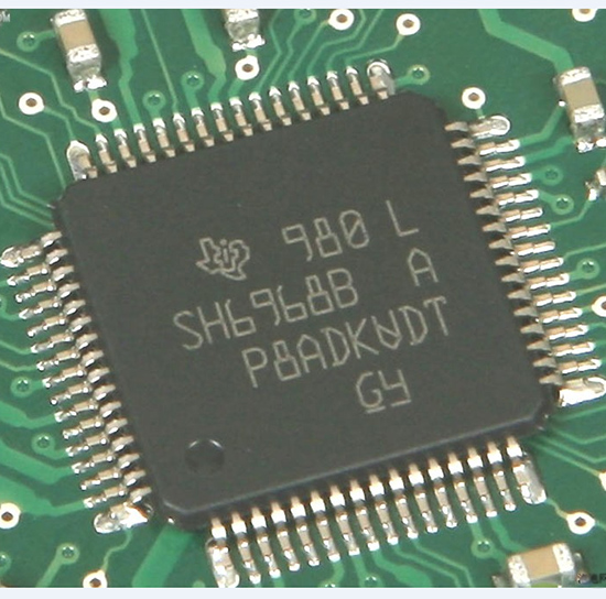
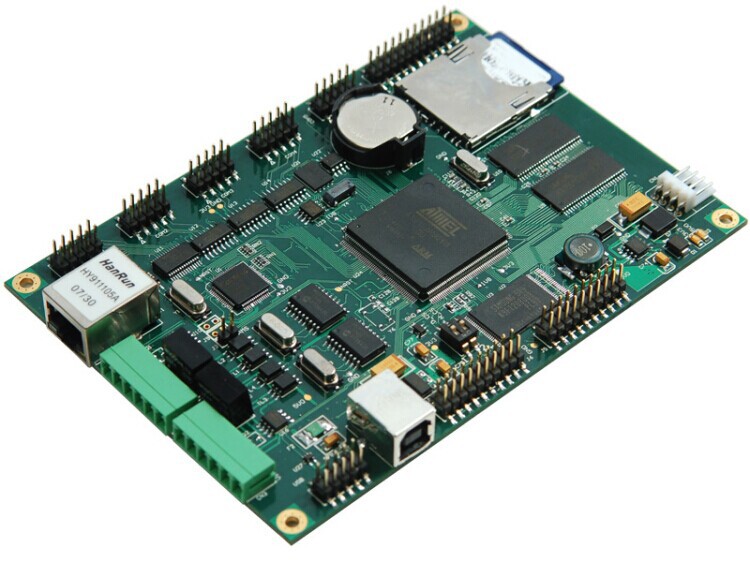
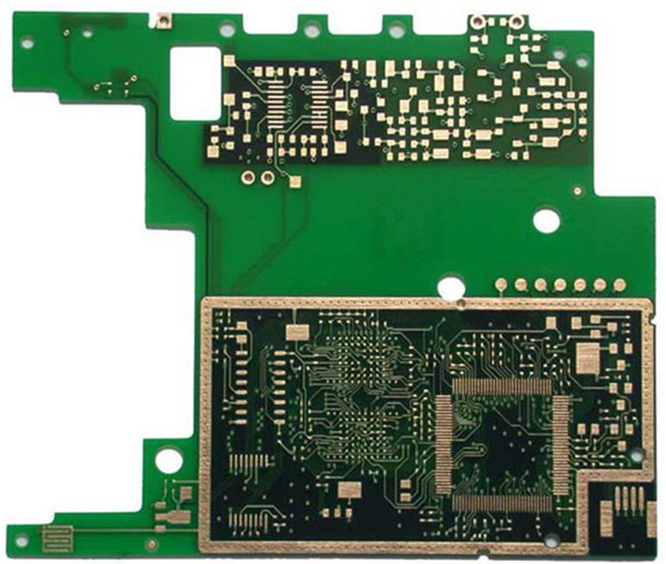
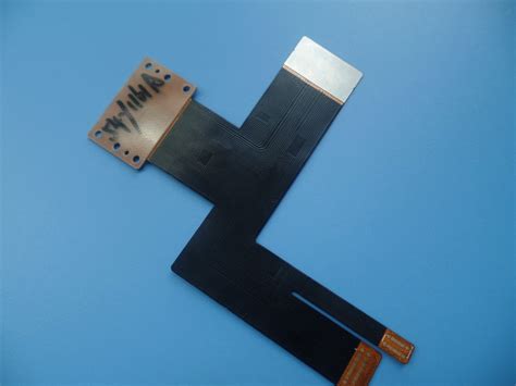
PCB board cloning samples: copper layer, solder mask and populated boards
PCB copy · board cloning

1 to 32 layers, including the boards other shops send back

Blind and buried vias, laser microvia HDI, RF microstrip, ceramic and flex substrates, fine pitch BGA. Every net is checked electrically against your sample, then a prototype is built and tested before any file leaves the building.

  • You receiveGerber, BOM, PCB source, placement
  • ProofWorking prototype, flying probe report
  • 1-2 layer, from$150
  • 4-6 layer, from$280
  • 8-10 layer, from$550
  • 10+ layer, HDI, RF, from$1,100
Also from the same engineering team

When a copy alone will not bring the machine back

Second service

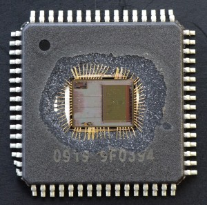
IC unlock, IC crack and chip decipher

Protected MCU, ARM, CPLD and FPGA parts read out through software attack, fault injection, side channel analysis or invasive microprobing, whichever the die calls for. Our database covers 5000+ models.

  • 8051, STC, Holtek, from$220
  • STM32 F0 / F1 / F3, from$700
  • ARM, Renesas, Infineon, from$2,000
You receive: Bin + Hex file, 2 programmed chips
See the IC unlock service
Third service

PCB reverse engineering

Schematic recovery for boards you need to change, not just repeat. Netlist extraction verified connection by connection, every part identified with a real manufacturer number, and editable source your own engineers can open.

  • Schematic + BOM, from$400
  • Prototype build and test, from$600
  • Typical lead time7-15 days
You receive: schematic, netlist, BOM with MPN, source files
See what gets recovered
Reverse engineering deliverables

Exactly what lands in your inbox

Ask any supplier this before you pay a deposit. Here is our answer in file formats, not adjectives.

  • GerberRS-274X, fab ready
  • PCB sourceAltium / PADS / Cadence
  • SchematicPDF + editable source
  • NetlistEvery connection, verified
  • BOMWith manufacturer part numbers
  • PlacementPick and place / coordinates
  • FirmwareBin and Hex
  • Samples2 programmed chips
  • Obsolescence notesDead parts and what replaces them
  • VerificationFlying probe + test report
Price and lead time

Published starting prices, so you can budget before you call

Service From Lead time
PCB copy — 1-2 layer $150 3-5 days
PCB copy — 4-6 layer $280 7-12 days
PCB copy — 8-10 layer $550 10-14 days
PCB copy — 10+ layer, HDI, RF, ceramic $1,100 12-15 days
Reverse engineering — schematic + BOM $400 7-15 days
IC unlock — 8051, STC, AT89, Holtek $220 2-4 days
IC unlock — STM32 F0 / F1 / F3 $700 3-5 days
IC unlock — ARM, Kinetis, Renesas, Infineon $2,000 7-15 days

Final price follows layer count, component density and chip package. Send a photo and you get the real number the same working day.

How a project runs

Four steps, and you can stop after any of them

  1. Free feasibility check

    Send photos of the board or the chip marking. Within 24 hours you know whether it can be done, how long, and what it costs.

  2. NDA, then ship the sample

    We sign first, you ship second. Courier details and our full registered address go to you in writing.

  3. Engineering and your test

    We copy the board, recover the schematic or read out the chip, then send samples. The balance is due after your own test passes.

  4. Files, and production if wanted

    Full file package delivered. SMT assembly, X-ray BGA inspection and flying probe testing are in house if you need boards built.

Where the risk sits

If we cannot do it, you pay nothing

Sending a board to a supplier on the other side of the world is a real risk. These five terms move most of it onto us, and they are in the quote you receive, not only on this page.

  • Feasibility assessed free, before you commit
  • 50% deposit, balance only after your test passes
  • Full refund if the sample boards or chips fail your test
  • NDA signed before anything ships
  • Your files are never reused, resold or shown
Recent work

Three boards, three reasons the original files were gone

6-layer industrial control board, immersion gold

6-layer industrial control board, immersion gold

  • Layers6
  • Parts480
  • Lead time11 days

The MCU vendor had gone out of business and the plant had two spare boards left. Firmware extracted, board cloned, line back in production.

Read the case
Medical instrument main board, obsolete ARM

Medical instrument main board, obsolete ARM

  • Layers8
  • Parts610
  • Lead time14 days

Service contract required 10 more years of spares. Schematic recovered so the customer could redesign around a part still in production.

Read the case
RF board, high frequency substrate

RF board, high frequency substrate

  • Layers4
  • Parts95
  • Lead time9 days

Impedance-controlled traces measured and rebuilt, then verified on a real board before the files were handed over.

Read the case
Capability

Boards other shops send back

Blind and buried vias, laser microvia HDI, RF and microstrip, ceramic substrate, high component density, EMC-critical telecom boards, 1 to 32 layers.

In-house SMT lines, X-ray BGA inspection and flying probe testing mean the file you receive has already been proven on a physical board, not only on screen.

  • Minimum trace / space3 mil
  • Via typesThrough, blind, buried
  • SubstratesFR-4, Rogers, ceramic, flex
  • InspectionX-ray BGA, AOI, flying probe
  • Package types read outDIP, SOP, QFP, QFN, BGA
Before you send an enquiry

Five questions we answer every day

Gerber files ready for any fab, a BOM with real manufacturer part numbers, placement data, the PCB source file, and a prototype we have already built and tested against your sample. Boards from 1 to 32 layers, starting at $150.

A copy reproduces the board exactly as it is and is faster and cheaper. Reverse engineering recovers the schematic so you can change something, which is what you need when a part has gone obsolete. Tell us the goal and we will say which one actually fits.

Our unlock database covers 5000+ models, and 126 of them across 28 families are published on the chip list page. If yours is not listed it usually still works, we just have not published it. Send the marking and the check is free.

You pay nothing. The feasibility check costs nothing and any deposit is returned in full. We say so early rather than late.

We sign an NDA before you ship. Files are returned or deleted on request after delivery, and nothing goes into a portfolio without written permission.

All questions

From the workshop

Notes on chips, boards and obsolete parts

Get a quote

Tell us what you are holding

Two photos of the board, or a chip marking, is enough to start. You get feasibility, lead time and price back within 24 hours, with no obligation to go further.

  • EmailJudy@4pcba.com
  • WhatsApp+8613600427328
  • HoursHigh-Tech PCB Reverse Engineering Serices

A clear photo of the marking usually removes one round of questions.

Judy answers personally, High-Tech PCB Reverse Engineering Serices. NDA available before you send any file.

WhatsApp Send board details