As technology keeps advancing more sophisticated chips are being produced. In our modern world, we now have different chips which include FPGA, MCU, and DSP amongst others. Electronic systems comprise chips which control and monitor their operations. These chips are indeed the brain behind electronic systems produced today.
However, chips usually have codes written on them. To access these codes, it is crucial to have a software source. The chips on the electronic system have a Lock or hardware lock which is always locked. To access such chips, there is a need to crack it.
What is an IC Crack?

The ICs of electronic systems are usually encrypted. IC Crack involves decrypting the IC code via the semiconductor reverse engineering. This process is also referred to as IC decryption or IC unlock.
After the IC has been cracked, a programmer will be able to read the IC program.
What are the Methods of Cracking an IC?
IC Crack is usually handled by professional IC Crack services, since this process is a delicate one. There are many approaches to achieve an IC Crack. Some of these approaches will be discussed below.
Software attacking
This method involves using processor communication interfaces or security holes in cryptograhic algorithms to crack ICs. It is a popular method of Cracking ICs adopted by a good number of IC Crack services.
For instance, this approach was used to attack the ATMEL AT89C microcontrollers that were built earlier. The cracker used the loopholes in the timing design of the operation. During this process, a self designed program was used and the attacker halted the erasing of the program memory data. The ATMELAT89C became non-encrypted and the programmer could read the on-chip program.
Electronic detection attacks
When there is a normal operation, the electronic detection attacks monitor the interface and power connections. The electromagnetic radiation characteristics are monitored in order to cause an attack. The power consumption changes as the microcontroller carries out different instructions since it is an active electronic device.
Due to this, the attacker analyzes and detects these changes in order to get critical information from the microcontroller. The attacker uses mathematical statistics and electronic measuring instruments to detect such changes.
UV attack method
This method converts an encrypted chip to a non-encrypted one by applying ultraviolet radiation on the chip. After this, a programmer will directly read the program. The UV attack method is a great one for OTP chips. This is because the only method to erase these chips is by using UV light. Therefore, the UV light helps in getting rid of the encryption.
A good number of OTP chips are unlocked by using the IV attack method. Some OTP chip ceramic packages feature quartz windows. UV light can be used to irradiate this IC type. It is necessary to open the chip if it is packaged in a plastic material. This will help to expose the wafer to UV light..
The basic decryption doesn’t include any cost since the encryption of this chip is poor. Therefore, this chip decryption comes very cheap. A good example is the decryption of the SONIX SN8P2511and Infine on SCM.
Error Generation Attack Technology
In this technology, there are processor errors caused by abnormal operating conditions. The processor makes it accessible and easy to cause attacks. Clock and voltage strikes are the most common errors generation technologies used in causing attacks.
It is possible to force the processor to carry out some incorrect operations by using high-voltage and low-voltage attacks. You can reset the protection circuitry by using a clock transition. This can be done without interfering with the secured information. For some processors, clock and power transitions can have a huge impact on decoding and carrying out a single instruction.
What do IC Crack Services do?
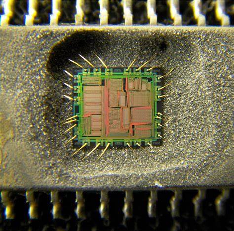
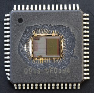
As it was earlier mentioned, IC Crack is usually carried out by IC Crack service providers. In most cases, they offer IC programs in Hex or Bin file. Also, they decap IC sample in such a way it won’t be functional again after breaking the IC.
Furthermore, some IC crack services offer unlockable models. The price of IC crack differs and as such, the right OC model needs to be sent in order to get a quotation. Some IC crack service providers accept half payment to commence a project. They begin IC crack when they have received sample payment. The second half of the payment is received after the project has been tested. A good number of IC crack service providers have strict rules guiding their payment and work.
Top 5 IC Crack Service Providers
There are many IC crack services available. Below are some of the best IC crack services you can rely on.
Well Done Technology
This IC crack service provider offers a lot of capabilities. Asides from IC unlock, they are into reverse engineering and PCB clones. Their technical team comprises professional engineers with great experience and skills. Well Done Technology offers reliable IC crack services. Their team gets program code from embedded chips like MCU, ARM, and DSP. Also, they map the printed circuit board in order to extract the PCB file and circuit diagram.
This IC crack service carries out research and analysis after acquiring the PCn circuit diagram and the chip program.
RayMing PCB
For some years now, RayMing PCB has carried out more than 1000 IC crack projects. They have got customers across different fields like telecom, healthcare, education, IT, and more. They provide their services to both start-ups and enterprises. This company is a highly preferred option for businesses interested in outsourcing their data processing and data entry operations.
At RayMing, some specific approaches are integrated for OC decryption. This company carries out the IC crack process with ultimate carefulness and precision. Also, the team here focuses on providing quality services to their customers.
OROD Technology Company
If you are in need of the right service provider to decrypt multi-layer PCB copy or high performance chip, OROD Technology Company has what it takes. The company which is located at Shenzhen provides IC crack service to many countries across the world. Also, they offer PCB clone services and have invested a lot of money on research. Customers have made good reviews about this company.
Shenzhen OROD has rich experience in IC crack and as such, offers 99 percent success rate when it comes to IV decryption. Their team of professional hardware and software engineers and integration of sophisticated technologies contributed to their great performance.
Shenzhen OROD technology promises their customers a competitive price and a very high success rate.
Fast PCB Studio
As one of the leading IC crack service providers in China, Fast PCB Studio is dedicated to offering a great solution for reverse engineering. With its headquarters in Dongguan, China, this company offers its services to customers across the world.
Apart from providing effective solutions for IC crack, Fast PCB Studio invests in research and development of multi-layer PCB reverse engineering. This reputable company offers 24-hour service to customers. Also, they provide IC decryption with a high success rate. They have got a team of dedicated professionals who crack IC for customers. This company unlocks IC chips before accepting payment from their customers.
Para Pardaz
Para Pardaz Company has a long standing experience in IC decryption. They have been able to crack the locks of many ICs. With the help of their highly skilled microelectronics engineers, this company has been able to perform exceedingly. These engineers are well inclined about the architecture and working principle of high-performance MCU. Also, they have a vivid understanding of the IC manufacturing process.
Para Pardaz can offer both IC crack and PCB reverse engineering services. They have continued to outperform some of their competitors because of their dedication to providing top-notch services.
Frequently Asked Questions
How much do IC crack service providers charge?
The cost of decrypting an IC usually varies among providers. Sometimes, cost varies based on the model. For instance an IC model can be more difficult to crack compared to others. Also, the type of provider you work with will determine how much you would be paying to crack your IC.
What type of file do customers get after IC crack has been performed?
A binary file is usually given to customers after IC crack. This file can burn through IC via a programmer. If customers are expecting an assembler code file, there is a need for a reverse compiling tool.
How do you choose an IC crack service provider?
When choosing an IC crack service provider, be sure to look out for some key factors. These factors include skills, technical knowhow, experience, and the type of IC crack method adopted. You can choose any of the above mentioned providers.
Conclusion
There are a lot of fake IC crack services out there who offer cheap prices in order to attract customers. These providers are after your money. Therefore, you need to take proper precaution when choosing an IC crack service provider. Remember you need a professional to crack your IC and as such, it is advisable to always go for quality.