Judy@4pcba.com
7:30 AM - 7:30 PM
Monday to Saturday

Archive: April 29, 2024

Laser Cut Framed Stencils

Introduction to Laser-Cut Stencils

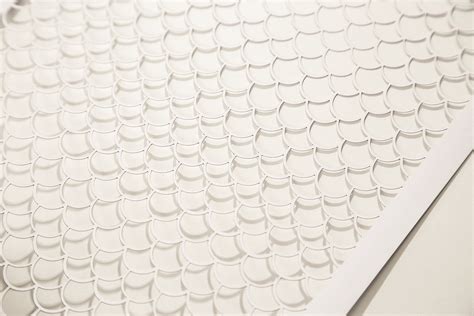
Laser-cut stencils have revolutionized the world of art and crafting, offering a precise and efficient method for creating intricate designs on various surfaces. These stencils are made using laser cutting technology, which allows for highly detailed and accurate cuts in a wide range of materials, including paper, plastic, wood, and metal. The versatility and precision of laser-cut stencils have made them popular among artists, crafters, and DIY enthusiasts alike.

What Are Laser-Cut Stencils?

Laser-cut stencils are templates created using a laser cutting machine. The machine uses a high-powered laser beam to cut through the chosen material, following a pre-programmed design. The result is a stencil with clean, precise edges that can be used to transfer the design onto another surface using paint, spray, or other mediums.

Advantages of Laser-Cut Stencils

Compared to traditional hand-cut stencils, laser-cut stencils offer several advantages:

  1. Precision: Laser cutting technology allows for intricate and detailed designs with clean, sharp edges.
  2. Consistency: Laser-cut stencils ensure that the design is consistently reproduced each time the stencil is used.
  3. Durability: Depending on the material used, laser-cut stencils can be more durable and long-lasting than hand-cut stencils.
  4. Efficiency: Laser cutting machines can produce stencils quickly and accurately, saving time and effort compared to hand-cutting.

Types of Materials for Laser-Cut Stencils

Laser-cut stencils can be made from a variety of materials, each with its own unique properties and advantages. Some of the most common materials used for laser-cut stencils include:

Paper and Cardstock

Paper and cardstock are affordable and easily accessible materials for creating laser-cut stencils. They are suitable for single-use or short-term projects and can be used with various mediums, such as paint, spray, and ink.

Plastic

Plastic stencils are more durable and reusable compared to paper stencils. They are ideal for projects that require multiple applications of the same design. Some common plastic materials used for laser-cut stencils include:

  • Mylar
  • Acetate
  • Polypropylene

Wood

Laser-cut wood stencils offer a unique, rustic appearance and are perfect for creating signs, wall art, and other decorative items. They can be used with paint, stain, or burn techniques to achieve various effects.

Metal

Metal stencils, such as stainless steel or brass, are extremely durable and long-lasting. They are suitable for industrial applications, such as marking and labeling, as well as for creating unique art pieces.

Designing Laser-Cut Stencils

Creating a design for a laser-cut stencil involves several steps and considerations. Here are some key aspects to keep in mind when designing your stencil:

Software and File Formats

To create a design for laser cutting, you’ll need to use vector-based software such as Adobe Illustrator, CorelDRAW, or Inkscape. These programs allow you to create scalable designs that can be easily adjusted and resized without losing quality. When saving your design, ensure that you use a compatible file format, such as AI, EPS, or SVG.

Design Considerations

When designing your laser-cut stencil, consider the following factors:

  1. Bridges and Islands: Ensure that your design has proper bridges (connections) between elements to prevent isolated islands (floating pieces) from falling out of the stencil.
  2. Line Thickness: Use appropriate line thicknesses to ensure that the laser cutter can accurately reproduce your design. Thin lines may not cut properly, while thick lines may result in a loss of detail.
  3. Negative Space: Remember that the negative space (the areas that will be cut out) in your design will be the parts that allow the medium to pass through and create the image on your surface.

Choosing a Laser Cutting Service

If you don’t have access to a laser cutter, you can use online laser cutting services to bring your stencil design to life. Some popular services include:

  • Ponoko
  • Sculpteo
  • Shapeways

When choosing a service, consider factors such as material options, pricing, turnaround time, and shipping costs.

Framing Laser-Cut Stencils

Framing your laser-cut stencils can enhance their durability, make them easier to handle, and provide a more professional appearance. Here are some methods for framing your stencils:

Wooden Frames

Wooden frames are a classic choice for framing stencils. They offer a sturdy and attractive option that can be customized to suit your style. To create a wooden frame for your stencil:

  1. Measure your stencil and cut four pieces of wood to create a frame that’s slightly larger than the stencil.
  2. Use wood glue and nails or screws to assemble the frame.
  3. Sand the frame and apply a finish, such as paint or stain, if desired.
  4. Attach your stencil to the back of the frame using adhesive or small nails.

Acrylic Frames

Acrylic frames provide a sleek, modern look for your laser-cut stencils. They are lightweight, durable, and easy to clean. To frame your stencil with acrylic:

  1. Measure your stencil and cut two pieces of acrylic to size – one for the front and one for the back.
  2. Use clear adhesive or double-sided tape to attach your stencil to the back piece of acrylic.
  3. Place the front piece of acrylic over the stencil and secure the edges with clear adhesive or tape.

Magnetic Frames

Magnetic frames are a versatile option that allows you to easily swap out stencils as needed. To create a magnetic frame:

  1. Cut a sheet of metal to the desired size of your frame.
  2. Attach magnets to the back of your stencil using adhesive.
  3. Place the stencil on the metal sheet, where it will be held in place by the magnets.

Applications and Projects

Laser-cut stencils can be used for a wide range of applications and projects, from home decor to professional signage. Here are some ideas to inspire your creativity:

Wall Art

Create unique wall art by using your laser-cut stencils to paint or spray designs onto canvas, wood, or directly onto your walls. Experiment with different colors, patterns, and layering techniques to achieve stunning results.

Fabric and Textile Designs

Use your stencils to create custom designs on fabric for clothing, pillows, curtains, or other textile projects. You can use fabric paint, bleach, or dye to transfer your designs onto the material.

Signage and Labeling

Laser-cut stencils are perfect for creating professional-looking signage and labels for businesses, events, or personal use. Use your stencils to paint or etch designs onto wood, metal, or plastic surfaces.

Decorative Items

Incorporate laser-cut stencils into your DIY projects to create unique decorative items, such as:

  • Coasters
  • Bookends
  • Trays
  • Plaques

Packaging and Branding

Use laser-cut stencils to add custom branding or designs to product packaging, business cards, or promotional materials. This can help create a cohesive and professional look for your business or personal brand.

Frequently Asked Questions (FAQ)

  1. Q: Can I create my own designs for laser-cut stencils?
    A: Yes, you can create your own designs using vector-based software such as Adobe Illustrator, CorelDRAW, or Inkscape. Ensure that your design is compatible with laser cutting by following the appropriate guidelines for line thickness, bridges, and islands.

  2. Q: How long do laser-cut stencils last?
    A: The durability of laser-cut stencils depends on the material used. Paper and cardstock stencils are suitable for single-use or short-term projects, while plastic, wood, and metal stencils can last for multiple uses and longer periods.

  3. Q: What is the best material for creating reusable laser-cut stencils?
    A: Plastic materials, such as Mylar or acetate, are ideal for creating reusable laser-cut stencils. They are durable, flexible, and easy to clean, making them suitable for multiple applications.

  4. Q: Can I use laser-cut stencils on any surface?
    A: Laser-cut stencils can be used on a variety of surfaces, including paper, fabric, wood, metal, and plastic. However, it’s essential to consider the compatibility of your chosen medium with the surface material to ensure the best results.

  5. Q: How do I clean my laser-cut stencils after use?
    A: To clean your laser-cut stencils, rinse them with warm water and mild soap, then gently scrub away any remaining paint or medium with a soft brush. Rinse the stencils again and allow them to air dry completely before storing or reusing them.

Conclusion

Laser-cut stencils offer a precise, efficient, and versatile way to create stunning designs on a wide range of surfaces. By understanding the materials, design considerations, and framing options available, you can unleash your creativity and produce professional-looking results for your art, crafting, or DIY projects. Whether you’re creating wall art, fabric designs, signage, or decorative items, laser-cut stencils provide endless possibilities for customization and personalization. So, embrace the power of laser cutting technology and start bringing your unique designs to life today!
HDI PCB – Which Stackup Type is Right for YRAYPCB

Introduction to HDI PCB Stackups

High-Density Interconnect (HDI) PCBs have become increasingly popular in recent years due to their ability to accommodate complex designs with high component density and miniaturization requirements. When designing an HDI PCB, selecting the appropriate stackup is crucial for ensuring optimal performance, manufacturability, and cost-effectiveness. In this article, we will explore the different types of HDI PCB stackups and provide guidance on choosing the right one for your specific needs.

What is an HDI PCB Stackup?

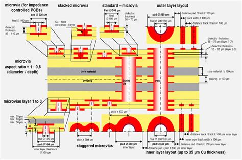
An HDI PCB stackup refers to the arrangement of conductive layers, dielectric materials, and vias within a printed circuit board. The stackup determines the electrical characteristics, signal integrity, and mechanical properties of the PCB. In HDI PCBs, the stackup typically involves thinner dielectric layers, smaller vias, and more complex routing compared to traditional PCBs.

Types of HDI PCB Stackups

There are several types of HDI PCB stackups, each with its own advantages and limitations. Let’s explore the most common types:

1. Microvia Stackup

Microvia stackups are the most widely used type of HDI PCB stackup. They utilize small, laser-drilled vias with diameters typically ranging from 50 to 150 microns. These vias connect the outer layers to the inner layers of the PCB, enabling high-density routing and component placement.

Advantages:
– Allows for high component density and miniaturization
– Enables efficient use of board space
– Provides good signal integrity and reduced crosstalk

Limitations:
– Higher manufacturing costs compared to traditional PCBs
– Requires specialized equipment and processes for fabrication

2. Buried Via Stackup

Buried via stackups involve placing vias within the inner layers of the PCB, rather than connecting the outer layers to the inner layers. This type of stackup is useful when there is limited space on the outer layers or when additional shielding is required between layers.

Advantages:
– Provides better signal integrity and reduced crosstalk
– Allows for more efficient use of board space
– Enables the creation of isolated power and ground planes

Limitations:
– Higher manufacturing costs due to additional processing steps
– Increased complexity in design and fabrication

3. Staggered Via Stackup

Staggered via stackups use a combination of microvias and buried vias to create a more complex interconnect structure. In this type of stackup, the vias are placed in a staggered pattern, allowing for higher routing density and improved signal integrity.

Advantages:
– Enables high-density routing and component placement
– Provides excellent signal integrity and reduced crosstalk
– Allows for more design flexibility and optimization

Limitations:
– Higher manufacturing costs due to the complexity of the stackup
– Requires careful design and planning to ensure manufacturability

4. Any Layer Via Stackup

Any layer via stackups allow for the placement of vias on any layer of the PCB, providing the highest level of design flexibility. This type of stackup is often used in highly complex designs where routing density and signal integrity are critical.

Advantages:
– Provides the highest level of design flexibility and optimization
– Enables high-density routing and component placement
– Offers excellent signal integrity and reduced crosstalk

Limitations:
– Highest manufacturing costs among HDI PCB stackups
– Requires advanced design skills and specialized fabrication processes

Choosing the Right HDI PCB Stackup

When selecting the appropriate HDI PCB stackup for your design, consider the following factors:

  1. Design Complexity: Evaluate the complexity of your design, including the number of components, routing density, and signal integrity requirements. More complex designs may require more advanced stackup types, such as staggered or any layer via stackups.

  2. Manufacturing Cost: Consider the manufacturing costs associated with each stackup type. Microvia stackups are generally the most cost-effective, while buried via, staggered via, and any layer via stackups involve higher costs due to additional processing steps and complexity.

  3. Board Size and Layer Count: The size of your PCB and the number of layers required will influence the choice of stackup. Smaller boards with fewer layers may benefit from microvia or buried via stackups, while larger and more complex boards may require staggered or any layer via stackups.

  4. Signal Integrity Requirements: Assess the signal integrity requirements of your design, including the need for controlled impedance, reduced crosstalk, and shielding. Buried via and staggered via stackups offer better signal integrity compared to microvia stackups.

  5. Manufacturing Capabilities: Consider the manufacturing capabilities of your chosen PCB fabrication partner. Some stackup types may require specialized equipment and processes that not all manufacturers can accommodate.

HDI PCB Stackup Comparison

To help you make an informed decision, here’s a comparison table of the different HDI PCB stackup types:

Stackup Type Advantages Limitations Typical Applications
Microvia – High component density
– Efficient board space use
– Good signal integrity
– Higher cost than traditional PCBs
– Requires specialized equipment
– Smartphones
– Wearable devices
– Internet of Things (IoT) devices
Buried Via – Better signal integrity
– Efficient board space use
– Isolated power and ground planes
– Higher cost due to additional processing
– Increased design complexity
– High-speed digital devices
– RF and microwave applications
– Automotive electronics
Staggered Via – High routing density
– Excellent signal integrity
– Design flexibility
– Higher cost due to stackup complexity
– Requires careful design planning
– High-performance computing
– Telecommunications equipment
– Medical devices
Any Layer Via – Highest design flexibility
– High routing density
– Excellent signal integrity
– Highest manufacturing cost
– Requires advanced design skills
– Aerospace and defense applications
– High-end consumer electronics
– Cutting-edge research and development

Frequently Asked Questions (FAQ)

  1. What is the main difference between HDI PCBs and traditional PCBs?
  2. HDI PCBs have smaller vias, thinner dielectric layers, and more complex routing compared to traditional PCBs, enabling higher component density and miniaturization.

  3. Can I use a microvia stackup for a high-speed digital design?

  4. While microvia stackups offer good signal integrity, buried via or staggered via stackups may be more suitable for high-speed digital designs due to their better signal integrity and reduced crosstalk.

  5. How do I determine the appropriate layer count for my HDI PCB?

  6. The layer count depends on the complexity of your design, routing requirements, and component placement. Work with your PCB design team and fabrication partner to determine the optimal layer count for your specific application.

  7. Are HDI PCBs more expensive than traditional PCBs?

  8. Yes, HDI PCBs generally have higher manufacturing costs compared to traditional PCBs due to the specialized equipment, processes, and materials required for their fabrication.

  9. What should I consider when choosing a PCB fabrication partner for my HDI design?

  10. When selecting a PCB fabrication partner, consider their experience with HDI PCBs, available manufacturing capabilities, quality control processes, and ability to meet your specific design requirements and timeline.

Conclusion

Choosing the right HDI PCB stackup is essential for achieving optimal performance, manufacturability, and cost-effectiveness in your PCB design. By understanding the different types of stackups and their advantages and limitations, you can make an informed decision based on your specific design requirements.

When in doubt, consult with your PCB design team and fabrication partner to determine the best stackup for your application. With careful planning and execution, HDI PCBs can help you push the boundaries of innovation and create cutting-edge electronic devices.

What Happened To HacknMod.com?

Introduction

In the early days of Android, HacknMod.com was one of the go-to destinations for Android enthusiasts looking to mod and customize their devices. The site provided a wealth of information, guides, and resources for rooting, installing custom ROMs, and tweaking Android to get the most out of it.

However, in recent years, HacknMod seemed to slowly fade away. Updates became less frequent, and eventually the site went offline altogether. So what exactly happened to this once-thriving community? Let’s take a look back at the history of HacknMod and explore the factors that may have led to its ultimate fate.

The Rise of HacknMod

Early Days

HacknMod.com was founded in 2010 by a group of Android enthusiasts who wanted to create a centralized resource for all things related to modding and customizing Android devices. At the time, the Android modding scene was still in its infancy, and there weren’t many established communities or websites dedicated to the topic.

HacknMod quickly gained popularity thanks to its detailed guides, helpful forums, and active community of modders. The site covered a wide range of topics, from rooting and unlocking bootloaders to installing custom ROMs and kernels.

Growth and Popularity

As Android’s user base grew, so did HacknMod’s audience. The site became a go-to resource for both novice and experienced modders alike. HacknMod’s guides were often cited and linked to from other Android sites and forums, further cementing its status as an authoritative source in the modding community.

During its peak, HacknMod had a thriving forum with thousands of active members. The forums were a place for users to ask questions, share tips and tricks, and showcase their modded devices. Many notable developers and modders got their start on HacknMod’s forums before going on to create popular custom ROMs and mods.

The Decline of HacknMod

Increased Competition

As Android continued to grow in popularity, so did the number of websites and communities dedicated to modding and customization. XDA Developers, in particular, emerged as a major player in the Android modding scene, with its massive forum and extensive library of guides and resources.

With more options available, some users began to drift away from HacknMod in favor of other communities. While HacknMod still had a dedicated core userbase, it became increasingly difficult for the site to attract new members and maintain its growth.

Changes in Android Modding

Over time, the Android modding landscape began to shift. With each new version of Android, Google introduced more restrictions and security measures that made it harder to mod and customize devices. Features like SafetyNet and Google’s certification process for Android devices made it more challenging for users to root and install custom ROMs without potentially losing access to certain apps and services.

As a result, the demand for traditional modding and customization began to wane. While there was still a niche audience for these kinds of mods, the mainstream Android userbase became less interested in tinkering with their devices on a low level.

Lack of Updates and Maintenance

As HacknMod’s popularity declined, so did the frequency of updates and new content on the site. Guides and tutorials became outdated as new Android versions were released, and the forums saw less activity as users moved on to other communities.

It’s unclear exactly why HacknMod’s owners and administrators stepped back from maintaining the site. It’s possible that they simply lost interest or motivation as the Android modding scene changed, or that they didn’t have the resources or time to keep the site updated and relevant.

The Offline Period and Attempted Revival

HacknMod Goes Offline

In 2018, HacknMod.com suddenly went offline without any explanation or announcement from the site’s owners. The site remained inaccessible for several months, leaving many users wondering what had happened and if HacknMod would ever return.

During this time, there was speculation within the Android community about the fate of HacknMod. Some users theorized that the site had been shut down due to legal issues or pressure from Google, while others believed that the owners had simply abandoned the project.

Attempted Revival and Ultimate Fate

In 2019, HacknMod briefly came back online with a message from the site’s owners stating that they were working on reviving and updating the site. However, this revival was short-lived, and HacknMod went offline again after only a few weeks.

Since then, there have been no further updates or announcements from HacknMod’s owners. The site remains offline, and it seems unlikely that it will ever return in its previous form.

While some users hold out hope for a potential revival, most have accepted that HacknMod is gone for good and have moved on to other communities and resources for their Android modding needs.

The Impact and Legacy of HacknMod

A Pioneering Android Modding Community

Despite its ultimate fate, it’s important to recognize the significant role that HacknMod played in the early days of Android modding. As one of the first major communities dedicated to Android customization, HacknMod helped to establish many of the practices, conventions, and resources that are still used by modders today.

HacknMod’s guides and tutorials served as a starting point for countless Android users who were interested in modding but didn’t know where to begin. The site’s active forums provided a space for modders to connect, collaborate, and share their knowledge and expertise.

Notable HacknMod Alumni

Over the years, HacknMod served as a launchpad for many notable developers and modders who went on to make significant contributions to the Android community. Some examples include:

Developer Notable Contributions
Chainfire Developer of SuperSU and various root-related tools
Koushik Dutta Creator of ClockworkMod Recovery and ROM Manager
Francisco Franco Developer of the popular Franco Kernel for Nexus devices

These developers, among many others, got their start on HacknMod’s forums and went on to create some of the most widely-used tools and mods in the Android community.

Lessons Learned from HacknMod’s Fate

The story of HacknMod serves as a reminder of the challenges and risks involved in running an online community, particularly one focused on a niche topic like Android modding.

As the Android modding scene evolved and became more complex, it likely became increasingly difficult for HacknMod’s owners to keep up with the demands of maintaining and updating the site. Without a clear succession plan or a way to generate sustainable revenue, the site was vulnerable to stagnation and eventual abandonment.

HacknMod’s fate also highlights the importance of adapting to changes in the broader ecosystem. As Android itself changed and became more secure, the demand for traditional modding and customization began to decline. Communities that were able to evolve and find new niches within the Android ecosystem were more likely to survive and thrive in the long run.

FAQ

Q: Is HacknMod.com ever coming back?

A: While there was a brief attempt to revive HacknMod in 2019, the site has remained offline since then with no further updates or announcements from the owners. At this point, it seems unlikely that HacknMod will return in its previous form.

Q: What happened to all the content and guides on HacknMod?

A: Unfortunately, when HacknMod went offline, much of its content and resources became inaccessible. Some guides and tutorials may have been archived or mirrored on other sites, but the vast majority of HacknMod’s content is no longer available.

Q: Are there any other Android modding communities similar to HacknMod?

A: While no site has directly replicated HacknMod’s exact format and community, there are several other notable Android modding communities that users have gravitated towards. XDA Developers is arguably the largest and most active, with forums dedicated to a wide range of devices and topics. Other popular communities include Android Forums, Android Central, and Reddit’s various Android-related subreddits.

Q: Is Android modding still popular today?

A: While the Android modding scene has evolved and changed over the years, there is still an active community of users who enjoy tinkering with and customizing their devices. However, the focus has shifted away from low-level mods like custom ROMs and kernels and towards more user-friendly customization options like launchers, icon packs, and Magisk modules.

Q: What can we learn from the story of HacknMod?

A: HacknMod’s rise and fall serves as a reminder of the challenges and risks involved in running an online community, particularly one focused on a niche topic. It also highlights the importance of adapting to changes in the broader ecosystem and having a clear plan for long-term sustainability and succession.

Conclusion

The fate of HacknMod.com is a bittersweet story in the history of Android modding. While the site may be gone, its impact and legacy live on through the developers, modders, and enthusiasts who got their start on its forums and used its resources to learn and grow.

As the Android modding scene continues to evolve and change, it’s important to remember the pioneers and trailblazers who helped to establish the community in its early days. HacknMod may be gone, but its spirit of curiosity, collaboration, and customization lives on in the countless users who continue to push the boundaries of what’s possible with Android.

HDI PCB Manufacturer– How to Choose the Right Manufacturer

What is an HDI PCB?

Before we dive into the specifics of choosing an HDI PCB Manufacturer, let’s first understand what HDI PCBs are. HDI PCBs are printed circuit boards that feature higher wiring density and smaller vias compared to traditional PCBs. They are designed to accommodate the increasing demand for miniaturization and enhanced performance in electronic devices.

HDI PCBs are characterized by the following features:

  • Fine line width and spacing (typically less than 100 microns)
  • Microvias (blind, buried, or stacked vias)
  • High layer count (usually 8 or more layers)
  • Thin core and prepreg materials

These features enable HDI PCBs to offer several benefits, such as:

  • Reduced size and weight of electronic devices
  • Improved signal integrity and electromagnetic compatibility
  • Higher component density and functionality
  • Enhanced thermal management

Factors to Consider When Choosing an HDI PCB Manufacturer

1. Technical Capabilities

When evaluating potential HDI PCB manufacturers, it is essential to assess their technical capabilities. Look for a manufacturer that has experience in producing HDI PCBs and possesses the necessary equipment and expertise to meet your specific requirements.

Consider the following technical aspects:

  • Manufacturing processes: The manufacturer should have a well-established and optimized manufacturing process for HDI PCBs, including advanced drilling, plating, and lamination techniques.
  • Equipment and technology: Ensure that the manufacturer has state-of-the-art equipment and employs the latest technologies to produce high-quality HDI PCBs consistently.
  • Material selection: The manufacturer should have access to a wide range of high-quality materials, including thin core and prepreg materials, to ensure the optimal performance of your HDI PCBs.
  • Design support: A good HDI PCB manufacturer should offer design support services to help you optimize your PCB layout and ensure manufacturability.

2. Quality Control and Certifications

Quality is paramount when it comes to HDI PCBs, as any defects or inconsistencies can lead to costly failures and delays. Therefore, it is crucial to choose an HDI PCB manufacturer that has robust quality control processes in place and holds relevant certifications.

Look for the following quality-related factors:

  • Quality management system: The manufacturer should have a well-documented and implemented quality management system, such as ISO 9001, to ensure consistent quality throughout the manufacturing process.
  • Testing and inspection: Ensure that the manufacturer employs rigorous testing and inspection procedures, including electrical testing, visual inspection, and automated optical inspection (AOI), to identify and rectify any defects.
  • Certifications: Verify that the manufacturer holds relevant certifications, such as UL, IPC, and RoHS, to demonstrate their commitment to quality and compliance with industry standards.
  • Traceability: The manufacturer should have a system in place to trace materials, processes, and products throughout the manufacturing cycle, enabling quick identification and resolution of any issues.

3. Cost and Lead Time

Cost and lead time are critical considerations when selecting an HDI PCB manufacturer. While it is important to obtain competitive pricing, it should not come at the expense of quality or reliability.

Consider the following aspects related to cost and lead time:

  • Pricing structure: Request quotations from multiple manufacturers and compare their pricing structures. Ensure that the quoted prices include all relevant costs, such as tooling, materials, and shipping.
  • Volume discounts: If you have high-volume requirements, inquire about volume discounts that can help reduce your overall costs.
  • Lead time: Discuss the manufacturer’s typical lead times for HDI PCBs and ensure that they can meet your project timelines. Consider factors such as production capacity, material availability, and shipping arrangements.
  • Rush services: In case of urgent requirements, check if the manufacturer offers rush services and understand the associated costs and feasibility.

4. Communication and Customer Support

Effective communication and responsive customer support are essential for a smooth and successful HDI PCB manufacturing experience. Look for a manufacturer that values open communication, transparency, and customer satisfaction.

Consider the following aspects of communication and customer support:

  • Responsiveness: The manufacturer should be prompt in responding to your inquiries, providing updates, and addressing any concerns you may have throughout the manufacturing process.
  • Technical support: Ensure that the manufacturer has a knowledgeable technical support team that can assist you with design reviews, manufacturability advice, and troubleshooting.
  • Language and cultural barriers: If you are considering an overseas manufacturer, assess their ability to communicate effectively in your preferred language and navigate any cultural differences.
  • Flexibility and adaptability: A good HDI PCB manufacturer should be flexible and adaptable to accommodate your specific requirements, such as design changes or delivery schedule adjustments.

5. Reputation and References

Researching the reputation and track record of potential HDI PCB manufacturers can provide valuable insights into their reliability, quality, and customer satisfaction. Seek references and feedback from industry peers, online forums, and professional networks.

Consider the following factors when evaluating a manufacturer’s reputation:

  • Customer testimonials: Look for customer testimonials or case studies that highlight the manufacturer’s capabilities, quality, and service.
  • Online reviews: Check online forums, social media, and review websites for feedback and experiences shared by other customers.
  • Industry presence: Assess the manufacturer’s presence and participation in industry events, publications, and associations, which can indicate their expertise and commitment to the field.
  • References: Request references from the manufacturer and reach out to them to gather first-hand information about their experience working with the manufacturer.

HDI PCB Manufacturing Process

Understanding the HDI PCB manufacturing process can help you better communicate your requirements and expectations to potential manufacturers. The typical HDI PCB manufacturing process involves the following steps:

  1. Design and Layout: The PCB design is created using specialized software, taking into account the specific requirements of HDI technology, such as fine line width, spacing, and microvia placement.

  2. Material Selection: The appropriate core and prepreg materials are selected based on the desired electrical, thermal, and mechanical properties of the HDI PCB.

  3. Drilling: High-precision drilling machines create the microvias and other holes in the PCB layers. Laser drilling is commonly used for HDI PCBs to achieve smaller via sizes.

  4. Plating: The drilled holes are plated with copper to create electrical connections between layers. Advanced plating techniques, such as via filling and stacking, are employed for HDI PCBs.

  5. Lamination: The individual PCB layers are stacked and laminated together under high pressure and temperature to form a solid board.

  6. Patterning: The desired circuit pattern is transferred onto the PCB surface through a photolithography process, followed by etching to remove the unwanted copper.

  7. Solder Mask and Silkscreen: A protective solder mask layer is applied to the PCB surface, and silkscreen markings are added for component placement and identification.

  8. Surface Finish: The exposed copper areas are coated with a surface finish, such as ENIG (Electroless Nickel Immersion Gold) or HASL (Hot Air Solder Leveling), to prevent oxidation and enhance solderability.

  9. Electrical Testing: The manufactured HDI PCBs undergo rigorous electrical testing to ensure proper functionality and adherence to specifications.

  10. Inspection and Packaging: The finished HDI PCBs are visually inspected for any defects, and then packaged and shipped to the customer.

Comparison of HDI PCB Manufacturers

To help you make an informed decision, let’s compare some of the leading HDI PCB manufacturers based on the key factors discussed earlier:

Manufacturer Technical Capabilities Quality and Certifications Cost and Lead Time Communication and Support
ABC PCB Inc. – Advanced HDI processes
– State-of-the-art equipment
– Experienced design support
– ISO 9001 certified
– UL and IPC certified
– Robust testing and inspection
– Competitive pricing
– Volume discounts available
– 2-3 weeks lead time
– Responsive customer service
– Multi-language support
– Flexible and adaptable
XYZ PCB Co. – Specialized in complex HDI designs
– Wide range of materials
– In-house design services
– ISO 9001 and ISO 14001 certified
– RoHS compliant
– 100% electrical testing
– Moderate pricing
– Rush services available
– 3-4 weeks lead time
– Online project tracking
– Dedicated account manager
– Proactive communication
123 PCB Ltd. – High-volume HDI manufacturing
– Automated assembly capabilities
– Rapid prototyping
– ISO 9001 and AS9100 certified
– IPC Class 3 certified
– Automated optical inspection
– Competitive high-volume pricing
– Flexible payment terms
– 4-5 weeks lead time
– 24/7 technical support
– Regular project updates
– Collaborative approach

Note: The information in the comparison table is for illustrative purposes only and does not represent any actual manufacturers.

Frequently Asked Questions (FAQ)

  1. What is the minimum line width and spacing for HDI PCBs?
  2. The minimum line width and spacing for HDI PCBs can vary depending on the manufacturer’s capabilities. Typically, HDI PCBs can achieve line width and spacing of 50-75 microns or less. However, it is essential to discuss your specific requirements with the manufacturer to ensure feasibility.

  3. How do I determine the appropriate layer count for my HDI PCB?

  4. The layer count for your HDI PCB depends on factors such as the complexity of your design, component density, signal integrity requirements, and power distribution needs. A good HDI PCB manufacturer should be able to review your design and provide recommendations on the optimal layer count based on your specific requirements.

  5. What are the common surface finish options for HDI PCBs?

  6. The most common surface finish options for HDI PCBs include ENIG (Electroless Nickel Immersion Gold), HASL (Hot Air Solder Leveling), and OSP (Organic Solderability Preservative). The choice of surface finish depends on factors such as solderability, durability, and compatibility with the components and assembly processes.

  7. How can I ensure the reliability of my HDI PCBs?

  8. To ensure the reliability of your HDI PCBs, choose a manufacturer that follows strict quality control processes, uses high-quality materials, and employs advanced manufacturing techniques. Additionally, consider incorporating design for manufacturability (DFM) principles, conducting thorough testing and inspection, and specifying appropriate environmental and operational requirements.

  9. What is the typical lead time for HDI PCB manufacturing?

  10. The lead time for HDI PCB manufacturing can vary depending on factors such as the complexity of the design, the manufacturer’s production capacity, and the order quantity. Typical lead times range from 2 to 5 weeks, but it is crucial to discuss your specific timeline requirements with the manufacturer and plan accordingly.

Conclusion

Choosing the right HDI PCB manufacturer is a critical decision that can significantly impact the success of your electronic product. By considering factors such as technical capabilities, quality control, cost, lead time, communication, and reputation, you can select a manufacturer that aligns with your specific needs and expectations.

Remember to thoroughly evaluate potential manufacturers, ask relevant questions, and seek references to make an informed decision. Building a strong partnership with your chosen HDI PCB manufacturer based on trust, transparency, and mutual understanding can lead to successful project outcomes and long-term business relationships.

As the demand for high-performance and miniaturized electronic devices continues to grow, HDI PCBs will play an increasingly essential role in the electronics industry. By partnering with the right HDI PCB manufacturer, you can leverage the benefits of this advanced technology to create innovative and competitive products that meet the evolving needs of your customers.

HDI PCB – The Ultimate Guide To How To Achieve A Perfect HDI

What is an HDI PCB?

HDI (High Density Interconnect) PCBs are printed circuit boards with a higher wiring density per unit area than conventional PCBs. This is achieved by incorporating thinner traces, smaller vias, and capture pads, and by using high-performance laminate materials.

HDI technology allows for denser component placement and more compact designs, enabling miniaturization of electronic devices. Some of the key characteristics of HDI PCBs include:

  • Trace widths and spaces less than 100 μm (4 mil)
  • Micro vias with diameters less than 150 μm (6 mil)
  • Pad diameters less than 400 μm (16 mil)
  • Thin copper foils and high-performance laminates

Benefits of HDI PCBs

HDI PCBs offer several advantages over traditional PCB designs:

  1. Space Savings: The compact nature of HDI PCBs allows for smaller form factors and higher component density, making them ideal for portable and handheld devices.

  2. Improved Signal Integrity: Shorter signal paths and reduced layer count in HDI designs lead to improved signal integrity and reduced electromagnetic interference (EMI).

  3. Enhanced Thermal Management: HDI PCBs can dissipate heat more efficiently due to the presence of microvias and buried vias, which act as thermal conduits.

  4. Cost Reduction: Although the initial setup costs for HDI PCBs may be higher, the overall cost can be lower due to reduced board size and layer count.

HDI PCB Design Considerations

When designing HDI PCBs, several factors must be taken into account to ensure optimal performance and manufacturability:

1. Layer Stack-up

The layer stack-up is a critical aspect of HDI PCB design. It determines the number of layers, their arrangement, and the interconnections between them. A typical HDI PCB Stack-up may include:

  • Signal layers
  • Ground and power planes
  • Microvia layers
  • Buried and blind vias

The choice of materials, layer thickness, and copper weights should be based on the specific requirements of the application, such as signal speed, impedance control, and thermal management.

2. Via Types and Sizes

HDI PCBs make use of various types of vias, each serving a specific purpose:

  • Through Vias: These are the most common type of vias, extending through all layers of the PCB.
  • Blind Vias: These vias are visible only on one side of the board and terminate at an inner layer.
  • Buried Vias: These vias are used to interconnect inner layers and are not visible on either side of the board.
  • Microvias: These are small, laser-drilled vias with diameters less than 150 μm, used for high-density interconnects.

The choice of via type and size depends on the design requirements, such as routing density, signal integrity, and manufacturability.

3. Trace Width and Spacing

HDI PCBs feature fine-pitch traces, with widths and spaces typically less than 100 μm (4 mil). The actual values depend on the PCB manufacturer’s capabilities and the specific design requirements.

When designing traces for HDI PCBs, consider the following:

  • Current-carrying capacity
  • Impedance control
  • Signal integrity
  • Manufacturability

Consult with your PCB manufacturer to determine the minimum trace width and spacing that can be reliably achieved.

4. Pad Size and Solder Mask Opening

Component pads on HDI PCBs are smaller than those on conventional PCBs, with diameters typically less than 400 μm (16 mil). The solder mask opening (SMO) should be designed to provide adequate clearance for the solder joint while preventing solder bridging.

The pad size and SMO depend on factors such as:

  • Component package type
  • Solder paste stencil thickness
  • Solder joint reliability requirements

Work closely with your PCB manufacturer and assembly house to ensure the pad design is optimized for the specific manufacturing process.

HDI PCB Manufacturing Process

The manufacturing process for HDI PCBs involves several specialized techniques and technologies:

1. Material Selection

HDI PCBs require high-performance laminate materials that offer:

  • Low dielectric constant and loss tangent
  • High thermal stability
  • Excellent mechanical properties
  • Compatibility with fine-pitch fabrication processes

Some common materials used for HDI PCBs include:

  • FR-4
  • Polyimide
  • PTFE (Teflon)
  • BT-epoxy
  • Ceramic

The choice of material depends on the specific application requirements, such as signal speed, thermal management, and cost.

2. Laser Drilling

Microvias in HDI PCBs are typically created using laser drilling. This process involves using a focused laser beam to create small, precise holes in the PCB substrate.

There are two main types of laser drilling:

  • UV laser drilling: This method uses ultraviolet laser light to create vias with diameters as small as 25 μm.
  • CO2 laser drilling: This method uses infrared laser light and is suitable for creating vias with diameters greater than 50 μm.

The choice of laser drilling method depends on the via size requirements and the capabilities of the PCB manufacturer.

3. Copper Plating

After the microvias are drilled, they are filled with copper to create electrical connections between layers. This is typically done using electroless and electrolytic copper plating processes.

The plating process involves the following steps:

  1. Cleaning and conditioning the via walls
  2. Applying a seed layer of copper using electroless plating
  3. Building up the copper thickness using electrolytic plating

The plating process must be carefully controlled to ensure uniform coverage and avoid voids or other defects.

4. Patterning and Etching

Once the copper plating is complete, the circuit pattern is created using photolithography and etching processes. This involves:

  1. Applying a photoresist layer to the copper surface
  2. Exposing the photoresist to UV light through a patterned mask
  3. Developing the photoresist to remove the unexposed areas
  4. Etching away the unwanted copper using a chemical etchant
  5. Stripping the remaining photoresist

The patterning and etching process must be optimized to achieve the fine feature sizes required for HDI PCBs.

HDI PCB Testing and Inspection

To ensure the quality and reliability of HDI PCBs, rigorous testing and inspection procedures are necessary. Some common methods include:

1. Automated Optical Inspection (AOI)

AOI uses high-resolution cameras and image processing software to detect surface defects such as:

  • Broken traces
  • Short circuits
  • Solder bridges
  • Missing components

AOI is a fast and efficient method for detecting visible defects, but it cannot identify internal issues.

2. X-Ray Inspection

X-ray inspection is used to detect internal defects in HDI PCBs, such as:

  • Voids in vias and solder joints
  • Misaligned or tilted components
  • Insufficient solder fill

X-ray inspection provides a non-destructive means of evaluating the internal structure of the PCB.

3. Electrical Testing

Electrical testing is used to verify the functionality and performance of the HDI PCB. This may include:

  • Continuity testing
  • Insulation resistance testing
  • High-potential (hipot) testing
  • Impedance testing

Electrical testing helps to ensure that the PCB meets the specified electrical requirements and is free from shorts, opens, or other faults.

FAQ

1. What is the minimum feature size achievable with HDI PCBs?

The minimum feature size depends on the specific capabilities of the PCB manufacturer. Typically, HDI PCBs can achieve trace widths and spaces less than 100 μm (4 mil), microvia diameters less than 150 μm (6 mil), and pad diameters less than 400 μm (16 mil).

2. Are HDI PCBs more expensive than traditional PCBs?

The initial setup costs for HDI PCBs may be higher due to the specialized equipment and processes required. However, the overall cost can be lower due to the reduced board size and layer count, which leads to material and assembly cost savings.

3. What are the main applications for HDI PCBs?

HDI PCBs are commonly used in applications that require high component density, miniaturization, and improved signal integrity. Some examples include:

  • Smartphones and tablets
  • Wearable electronics
  • Medical devices
  • Aerospace and defense systems
  • High-speed networking equipment

4. Can HDI PCBs be used for high-power applications?

While HDI PCBs are primarily designed for high-speed and high-density applications, they can be used for high-power applications with proper design considerations. This may involve the use of thicker copper layers, specialized materials, and enhanced thermal management techniques.

5. How can I ensure the manufacturability of my HDI PCB design?

To ensure the manufacturability of your HDI PCB design, follow these best practices:

  • Consult with your PCB manufacturer early in the design process
  • Adhere to the manufacturer’s design guidelines for minimum feature sizes and clearances
  • Use standard via sizes and pad shapes whenever possible
  • Perform thorough design rule checks (DRC) and manufacturability audits
  • Provide clear and accurate documentation, including Gerber files, drill files, and assembly drawings

By working closely with your PCB manufacturer and following industry best practices, you can achieve a perfect HDI PCB design that meets your performance, reliability, and cost requirements.

What Is The Core Of A Custom Drone Board

Key Components of a Drone Control Board

A typical drone main board integrates the following core subsystems:

  • Flight controller (FC)
  • Electronic speed controllers (ESCs)
  • Radio control receiver
  • Telemetry radio
  • GPS module
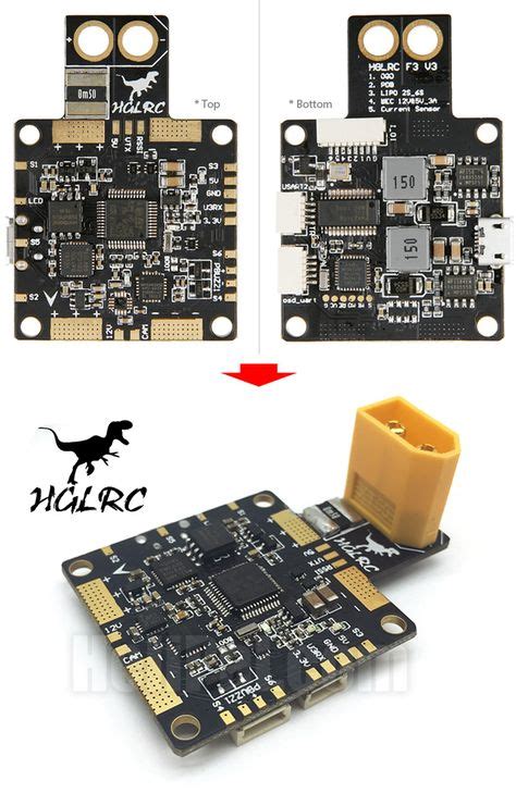
  • Power distribution board (PDB)
  • Sensors (accelerometer, gyro, barometer, etc.)

Let’s examine each of these components in more detail.

Flight Controller

The flight controller is the main processor that runs the software responsible for controlling the drone’s motion and stabilization. It takes inputs from the radio receiver, onboard sensors, and any autonomous navigation systems, and sends corresponding control signals to the ESCs and motors.

Some of the most popular open source flight controller firmware options include:

Firmware Description
Ardupilot Powerful, highly configurable autopilot supporting many vehicle types
Betaflight Optimized for smooth, responsive flight characteristics in racing/freestyle drones
PX4 Professional grade autopilot with wide range of advanced features
INAV Navigation-focused firmware with good GPS integration

Choosing the right flight controller and firmware depends on the specific requirements and goals for your custom drone build.

Electronic Speed Controllers

ESCs are responsible for converting the low current control signal from the flight controller into the high current 3-phase AC power that drives the brushless motors. For a quadcopter, 4 ESCs are required, one for each motor. Larger designs like hexacopters and octocopters will require 6 or 8 ESCs respectively.

The key factors to consider when selecting ESCs are:
– Maximum continuous current rating
– Supported protocols (PWM, Oneshot, Multishot, DShot, etc.)
– Size and weight
– Programmability

Ensuring the ESCs are appropriately sized for the motor stator size and propeller dimensions is critical. Overloaded ESCs can overheat and fail, potentially causing a dangerous crash.

Radio Control Receiver

The radio receiver allows the drone to be controlled remotely by the pilot. It communicates with the hand-held transmitter and translates the control stick inputs into signals that are fed into the flight controller. This is what enables real-time flying and maneuvering of the drone.

The most common frequencies for RC drone control are:
– 2.4 GHz
– 433 MHz (for long range)
– 900 MHz (for long range)

There are also various communication protocols used between the transmitter and receiver, such as:
– PWM
– PPM
– SBUS
– iBUS

Many receivers now support multiple protocols, making them compatible with a wider range of transmitters. This is helpful as it allows more flexibility and options when choosing a controller.

Telemetry Radio

In addition to the main RC link, most drones also incorporate a separate telemetry radio system. This allows for real-time transmission of flight data from the drone back to the pilot’s ground station. Common telemetry data includes:
– Battery voltage and current draw
– GPS coordinates and altitude
– Flight controller status
– Sensor readings
– Informational messages and error codes

Having access to this live data stream can be extremely valuable when monitoring the health and performance of the drone in flight. It provides an early warning if something starts to go wrong, potentially allowing the pilot to take corrective action before a failure occurs.

Some of the most widely used telemetry systems are:
– 3DR Radio
– DragonLink
– FrSky
– LightTelemetry
– XBee

The choice of telemetry system will depend on the desired range, data bandwidth, and compatibility with other components.

GPS Module

For any autonomous or assisted flight modes, a GPS module is a must. It provides the drone with accurate position and velocity data that can be used for navigation and stabilization. Standard GPS is accurate to within a few meters, but some higher end modules can achieve centimeter level precision by using Real Time Kinematic (RTK) techniques.

Important considerations when choosing a GPS module include:
– Satellite constellations supported (GPS, GLONASS, BeiDou, Galileo)
– Update rate
– Horizontal and vertical position accuracy
– Time to first fix
– Size and weight

Typically the GPS will connect to a dedicated port on the flight controller, and may also require a separate power supply. The FC firmware will have specific configuration settings for adjusting the GPS parameters.

Power Distribution Board

The PDB is responsible for taking the battery voltage and safely distributing it to the ESCs and other components. It also often includes power filtering capacitors, voltage regulators for 5V and 12V peripherals, and current sensing for battery monitoring.

Key design considerations for the PDB include:
– Maximum total current capability
– ESC power connectors
– Additional auxiliary power connectors
– Voltage regulators
– Current sensor
– Size and layout

Some PDBs may also include the battery eliminator circuit (BEC) used to power the FC, receiver, and servos. However, many builders prefer to use separate standalone BEC modules for improved reliability.

Sensors

In order to fly stably, the drone needs to have accurate data about its orientation and motion. This is where the onboard sensor suite comes in. The core sensors found on most flight controllers include:

Sensor Function
Accelerometer Measures linear acceleration forces, used for determining orientation
Gyroscope Measures angular velocity, used for tracking rotation
Barometer Measures air pressure, used for altitude hold
Magnetometer Measures Earth’s magnetic field, used as a compass for navigation

By fusing the data from these different sensors, the flight controller can determine the drone’s absolute orientation in space. This is crucial for self-leveling and executing autonomous maneuvers.

Additional sensors that may be helpful for more advanced applications include:

  • Optical flow camera
  • Laser rangefinder
  • Ultrasonic rangefinder
  • Precision landing beacon detector

The choice of sensors will be dependent on the specific use case and performance requirements for the drone.

Choosing a Flight Controller

With so many different flight controllers on the market, it can be difficult to know where to start. Here are some key factors to consider when making a selection:

Microprocessor

The “brain” of the flight controller is the main processor chip. It needs to be fast enough to run the stabilization loops and navigation algorithms in real-time. Some common choices are:

  • STM32F4
  • STM32F7
  • STM32H7

In general, the higher the processor speed, the better the flight performance will be. However, this also comes at the cost of increased power consumption and heat generation.

Firmware Compatibility

In order to actually fly, the hardware needs to be loaded with compatible firmware. It’s important to check that the flight controller supports the desired firmware and version.

For example, Betaflight is optimized for STM32F4 and STM32F7 based controllers. It will not run on an STM32F3 board. Similarly, a newly released FC may not yet be supported by an older firmware version. Always consult the documentation and compatibility charts before making a purchase.

Form Factor

Flight controllers come in a range of different physical form factors. Some of the most common are:

  • 30.5mm x 30.5mm (standard size)
  • 20mm x 20mm (mini size)
  • 16mm x 16mm (micro size)

Smaller sizes can be advantageous for tight builds, but may sacrifice features or expandability. It’s also important to consider the mounting hole layout and stack height when selecting a form factor.

Sensor Suite

As discussed earlier, the onboard sensors are a key part of any flight controller. Higher end FCs will often use more sophisticated sensors with better noise performance and temperature stability.

Some controllers come with barometer and magnetometer sensors built-in, while others will require external modules to be connected. Consider the specific needs of your build when deciding which sensors are required.

Connectivity

Pay close attention to the types and number of ports available on the FC. Ensure that there are enough connections for all the peripherals you plan to use, such as:

  • RC receiver
  • ESCs
  • GPS
  • Telemetry
  • Blackbox logging
  • Additional sensors
  • LED strip
  • Buzzer
  • etc.

If the FC doesn’t have enough ports, you may need to use breakout boards, splitters, or other adapters. This can add complexity and points of failure to the wiring.

Price

Of course, budget is always a consideration in any project. Flight controller prices can range from around $20 for a basic model up to $200 or more for high end units.

In general, you get what you pay for. More expensive controllers will offer better performance, more features, and higher quality components. However, it’s not always necessary to go for the top of the line option. Many cheaper FCs are still perfectly capable of delivering great flight characteristics.

The key is to strike a balance between price and performance that makes sense for your specific needs. Don’t overspend on features you’ll never use, but also don’t skimp too much on quality or you may end up regretting it later.

Integrated vs Modular Design

One important decision when designing a custom drone is whether to go with an integrated or modular architecture. An integrated approach combines the FC, ESCs, PDB, and sometimes even the RC receiver into a single PCB. A modular design uses separate boards for each function, which are then wired together.

Integrated Pros:

  • Simpler wiring with fewer connections
  • Lighter weight
  • More compact
  • Lower cost

Integrated Cons:

  • Limited upgrade options
  • Harder to repair/replace individual components
  • Less flexibility in component choice

Modular Pros:

  • Easily upgradeable
  • Components can be swapped out as needed
  • More customization options
  • Damaged components can be replaced individually

Modular Cons:

  • More complex wiring with more failure points
  • Heavier
  • Physically larger
  • Higher cost

The best approach depends on the specific goals and constraints of the build. An integrated design may be preferred for a racing drone where every gram counts. A modular approach may be better for a large photography platform where easy maintenance is important.

Firmware Options

As mentioned previously, there are several different firmware options available for drone flight controllers. Each has its own strengths, weaknesses, and unique features. Let’s take a closer look at some of the most popular choices.

Ardupilot

Ardupilot is a powerful open source autopilot system that can control almost any type of vehicle, from multirotors to fixed wing planes to cars and boats. It has a wide range of advanced features and customization options.

Some of the key capabilities include:
– Waypoint navigation
– Mission planning
– Autonomous landing
– Camera control
– Follow-me mode
– Geofencing
– Acro/stabilize/loiter/guided/auto flight modes

Ardupilot is a great choice for anyone looking to build a fully autonomous drone for mapping, surveying, or other professional applications. It does have a bit of a learning curve, but the extensive documentation and active community make it relatively easy to get started.

Betaflight

Betaflight is a popular firmware choice for FPV racing and freestyle drones. It is known for its exceptional flight performance and responsiveness. The firmware is highly optimized for fast control loops and low latency.

Some standout features of Betaflight include:
– Oneshot/Multishot/DShot ESC protocols for faster motor updates
– Configurable PID controllers for fine-tuning flight behavior
– Blackbox logging for recording high-rate flight data
– Dynamic filters for smoother motor control
– Configurable stick commands and mode switches

While Betaflight is an excellent performer, it can be a bit daunting for new users. The sheer number of settings and options can be overwhelming. It’s recommended to start with one of the prebuilt configuration files and only make small tweaks until you’re more comfortable with the system.

PX4

PX4 is another popular open source autopilot firmware. It is designed for professional and industrial applications that require maximum reliability and safety. Some of the key features include:

  • Extensive sensor compatibility, including RTK GPS and precision landing
  • Advanced computer vision integration
  • Detailed system monitoring and logging
  • Simulation-in-Hardware and Software-in-the-Loop testing
  • Modular architecture for easy customization

PX4 is trusted by many commercial drone companies and has been used in a wide variety of applications from delivery to search and rescue. It is a great choice for anyone building a mission-critical platform that needs to meet high standards of safety and reliability.

However, it is overkill for most hobbyist projects. The advanced features and complex architecture come at the cost of increased resource requirements and configuration complexity.

INAV

INAV is an autopilot firmware that is specifically designed for GPS-guided autonomous flight. It includes a variety of advanced navigation modes and sensor integrations.

Some of the standout features of INAV include:

  • Excellent GPS performance for position hold and waypoint navigation
  • Dedicated modes for aerial photography like position hold and waypoint missions
  • Robust failsafe logic with configurable actions
  • Compatibility with a wide range of sensors including optical flow and laser rangefinders

INAV is a good choice for anyone building a drone for autonomous photography or videography. The navigation modes make it easy to capture smooth, stable footage without needing expert flying skills.

Like Ardupilot, it has a bit of a learning curve but is generally easier to configure than PX4. The documentation and community support are also very good.

FAQ

What is the best flight controller for a beginner?

For someone just starting out, it’s recommended to choose a FC with well-established firmware like Betaflight or INAV. Look for a controller with built-in sensors, a well-documented feature set, and good community support. Popular beginner-friendly options include the Matek F405, Omnibus F4, and Kakute F7.

How important is vibration isolation for the flight controller?

Proper vibration isolation is critical for preventing “noise” in the accelerometer and gyro data. This can lead to poor flight performance, “twitches”, and even complete loss of control. Always use high quality soft-mount grommets or standoffs to decouple the FC from frame vibrations. For especially noisy setups, an additional vibration-dampening plate may be necessary.

What are the differences between F1, F3, F4, and F7 processors?

The number designation for STM32 processors indicates the relative performance and capability. F1 is the oldest and slowest, while F7 is the newest and fastest. F3 and F4 are in between. In general, it’s best to select the most recent processor that is compatible with the desired firmware.

Can I use a flight controller with a built-in PDB?

Yes, there are many all-in-one flight controllers that integrate the PDB functionality. This can simplify wiring and reduce weight. However, it’s important to check that the power handling capabilities are sufficient for your motor and ESC combination. Also, consider that if either the PDB or FC fails, the entire board will need to be replaced.

What is the advantage of using an external magnetometer?

Many lower cost flight controllers have the magnetometer sensor built-in. However, this can be problematic as the nearby electrical currents from the motors and ESCs can interfere with the magnetic field readings. This can lead to poor yaw stability and inaccurate heading hold. Using an external magnetometer that is mounted away from the electronics can provide much better performance in these cases.

Conclusion

The flight controller is the core of any custom drone build. It serves as the central hub that integrates all the various components and subsystems. When designing a drone from scratch, it’s important to choose a FC that is well-suited to the specific goals and requirements of the project.

By understanding the key elements that go into a flight controller, you can make informed decisions about processor performance, sensor selection, firmware options, and physical form factor. It’s also important to consider whether an integrated or modular architecture makes more sense for your application.

Ultimately, the perfect flight controller will depend on a variety of factors. But by carefully evaluating the options and tradeoffs, you can design a system that delivers the capabilities and performance you need to bring your custom drone vision to life.

11 Things We Need to Know about PCB Programming and Testing Tools

Introduction to PCB Tools

Printed Circuit Board (PCB) design and manufacturing is a complex process that requires specialized tools for programming and testing. These tools are essential for ensuring the functionality, reliability, and quality of PCBs. In this article, we will explore 11 crucial aspects of PCB programming and testing tools that every electronics engineer and PCB designer should know.

1. PCB Design Software

1.1 Schematic Capture Tools

Schematic capture tools are used to create the initial design of a PCB. These tools allow designers to create a visual representation of the circuit, including components, connections, and net labels. Popular schematic capture tools include:

  • Altium Designer
  • OrCAD Capture
  • Eagle

1.2 PCB Layout Tools

Once the schematic is complete, PCB layout tools are used to create the physical design of the board. These tools allow designers to place components, route traces, and define board dimensions. Some well-known PCB layout tools are:

  • Altium Designer
  • Cadence Allegro
  • Mentor Graphics PADS

1.3 3D Visualization Tools

3D visualization tools provide a realistic representation of the PCB, allowing designers to check for potential issues such as component clearance and mechanical fit. Examples of 3D visualization tools include:

  • Altium Designer 3D
  • Autodesk Fusion 360
  • SolidWorks PCB

2. PCB Simulation Tools

2.1 Signal Integrity Simulation

Signal integrity simulation tools analyze the behavior of electrical signals on a PCB. These tools help designers optimize trace routing, impedance matching, and termination to ensure signal quality and minimize issues like crosstalk and reflections. Some popular signal integrity simulation tools are:

  • Ansys HFSS
  • Mentor Graphics HyperLynx
  • Cadence Sigrity

2.2 Power Integrity Simulation

Power integrity simulation tools evaluate the power distribution network on a PCB. They help designers optimize the placement of power and ground planes, decoupling capacitors, and voltage regulators to maintain stable power supply and minimize noise. Examples of power integrity simulation tools include:

  • Ansys SIwave
  • Cadence Sigrity PowerDC
  • Mentor Graphics HyperLynx PI

2.3 Thermal Simulation

Thermal simulation tools analyze the heat distribution on a PCB and help designers identify potential thermal issues. These tools allow designers to optimize component placement, heatsink design, and airflow to ensure proper thermal management. Some thermal simulation tools are:

  • Ansys Icepak
  • Mentor Graphics FloTHERM
  • Cadence Celsius

3. PCB Manufacturing Tools

3.1 Computer-Aided Manufacturing (CAM) Tools

CAM tools generate the necessary files for PCB manufacturing, such as Gerber files, drill files, and pick-and-place files. These tools ensure that the PCB design is accurately translated into the manufacturing process. Examples of CAM tools include:

  • Altium Designer CAM Editor
  • Cadence Allegro PCB Editor
  • Mentor Graphics Fablink

3.2 Gerber Viewers

Gerber viewers are used to inspect and verify the generated Gerber files before sending them to the PCB manufacturer. These tools help designers catch any errors or discrepancies in the manufacturing files. Some popular Gerber viewers are:

  • GC-Prevue
  • ViewMate
  • Ucamco UcamX

4. PCB Assembly Tools

4.1 Pick-and-Place Machines

Pick-and-place machines automate the process of placing components on a PCB. These machines use the generated pick-and-place files to accurately position components on the board. Examples of pick-and-place machine manufacturers include:

  • Fuji
  • Panasonic
  • Juki

4.2 Reflow Ovens

Reflow ovens are used to solder surface mount components onto the PCB. These ovens follow a specific temperature profile to melt the solder paste and create a reliable connection between the components and the board. Some popular reflow oven manufacturers are:

  • Heller
  • BTU
  • Rehm

4.3 Automated Optical Inspection (AOI) Systems

AOI systems use cameras and image processing algorithms to inspect the assembled PCB for defects such as missing components, incorrect component placement, and solder bridges. These systems help ensure the quality and consistency of the assembly process. Examples of AOI system manufacturers include:

  • Koh Young
  • Omron
  • Saki

5. PCB Testing Tools

5.1 In-Circuit Testing (ICT) Systems

ICT systems test the assembled PCB for manufacturing defects by directly probing the board’s nodes and components. These systems can detect issues such as short circuits, open circuits, and component value deviations. Some popular ICT system manufacturers are:

  • Keysight Technologies
  • Teradyne
  • Digitaltest

5.2 Flying Probe Testing Systems

Flying probe testing systems use movable probes to test the PCB without the need for a dedicated test fixture. These systems offer flexibility and are suitable for low-volume production or prototypes. Examples of flying probe testing system manufacturers include:

  • Takaya
  • Seica
  • Acculogic

5.3 Functional Testing Systems

Functional testing systems verify the PCB’s functionality by simulating real-world operating conditions. These systems can test the board’s inputs, outputs, and communication interfaces to ensure proper operation. Functional testing systems are often custom-built for specific applications.

6. PCB Programming Tools

6.1 In-System Programming (ISP) Tools

ISP tools allow designers to program microcontrollers and flash memories directly on the PCB without removing them from the board. These tools use various communication protocols, such as JTAG, SPI, or I2C, to access and program the devices. Some popular ISP tool manufacturers are:

  • Segger
  • PEmicro
  • Atmel (now part of Microchip)

6.2 Boundary Scan Testing Tools

Boundary scan testing tools use the JTAG interface to test the interconnections and functionality of components on a PCB. These tools can detect manufacturing defects and perform functional testing without the need for physical access to the board’s nodes. Examples of boundary scan testing tool manufacturers include:

  • XJTAG
  • JTAG Technologies
  • Corelis

7. PCB Rework and Repair Tools

7.1 Soldering Stations

Soldering stations are used for manual soldering and rework of PCBs. These stations typically include a soldering iron, a hot air gun, and a desoldering tool to facilitate the removal and replacement of components. Some well-known soldering station manufacturers are:

  • Weller
  • Hakko
  • Metcal

7.2 Rework Systems

Rework systems are specialized tools designed for the precise removal and replacement of surface mount components on a PCB. These systems often include a heating element, a vision system, and a placement mechanism to ensure accurate and reliable rework. Examples of rework system manufacturers include:

  • Metcal
  • Pace
  • Ersa

8. PCB Design Collaboration Tools

8.1 Version Control Systems

Version control systems help manage changes to PCB design files and facilitate collaboration among team members. These systems track revisions, allow for branching and merging, and provide a clear history of design changes. Some popular version control systems for PCB design are:

  • Git
  • Subversion (SVN)
  • Perforce

8.2 Design Review Tools

Design review tools enable team members to review and provide feedback on PCB designs. These tools often include features such as markup, commenting, and task assignment to streamline the review process. Examples of design review tools include:

  • Altium 365
  • Cadence Design Collaboration
  • Mentor Graphics PADS Collaborate

9. PCB Documentation Tools

9.1 Schematic and Layout Documentation Tools

Schematic and layout documentation tools generate comprehensive documentation for PCB designs, including schematic diagrams, bill of materials (BOM), and assembly drawings. These tools help ensure that the design is properly documented and communicated to stakeholders. Some popular documentation tools are:

  • Altium Draftsman
  • Cadence PCB Editor
  • Mentor Graphics Xpedition

9.2 Technical Writing Tools

Technical writing tools are used to create user manuals, application notes, and other technical documents related to PCBs. These tools often include features such as templating, version control, and collaborative editing. Examples of technical writing tools include:

  • Adobe FrameMaker
  • MadCap Flare
  • Oxygen XML Editor

10. PCB Data Management Tools

10.1 Component Libraries

Component libraries store and manage the data associated with electronic components used in PCB designs. These libraries include information such as schematic symbols, footprints, and 3D models. Some popular component library management tools are:

  • Altium Vault
  • Cadence OrCAD CIS
  • Mentor Graphics Library Manager

10.2 Design Data Management (DDM) Systems

DDM systems provide a centralized repository for storing and managing PCB design data, including schematic files, layout files, and manufacturing outputs. These systems help ensure data integrity, version control, and collaboration among team members. Examples of DDM systems include:

  • Altium Vault
  • Cadence OrCAD EDMS
  • Mentor Graphics EDM

11. Continuing Education and Resources

11.1 Online Learning Platforms

Online learning platforms offer courses and tutorials on various aspects of PCB design, programming, and testing. These platforms provide a convenient way for engineers to enhance their skills and stay up-to-date with the latest tools and techniques. Some popular online learning platforms for PCB-related topics are:

  • Udemy
  • Coursera
  • LinkedIn Learning

11.2 Professional Organizations and Conferences

Professional organizations and conferences provide opportunities for networking, knowledge sharing, and learning about the latest advancements in PCB technology. Some notable organizations and conferences in the PCB industry include:

  • IPC (Association Connecting Electronics Industries)
  • PCB West
  • DesignCon

Frequently Asked Questions (FAQ)

1. What is the difference between schematic capture and PCB layout tools?

Schematic capture tools are used to create a visual representation of the circuit, including components, connections, and net labels. PCB layout tools, on the other hand, are used to create the physical design of the board, including component placement, trace routing, and board dimensions.

2. Why are simulation tools important in PCB design?

Simulation tools help designers analyze and optimize various aspects of PCB performance, such as signal integrity, power integrity, and thermal management. By using simulation tools, designers can identify and resolve potential issues before the board is manufactured, saving time and costs associated with redesigns and rework.

3. What are the benefits of using automated testing tools for PCBs?

Automated testing tools, such as in-circuit testing (ICT) systems and flying probe testing systems, help ensure the quality and consistency of PCBs by detecting manufacturing defects and verifying the board’s functionality. These tools can significantly reduce the time and effort required for manual testing and improve the overall reliability of the final product.

4. How do version control systems facilitate collaboration in PCB design?

Version control systems allow team members to work on PCB design files simultaneously, track changes, and manage revisions. These systems provide a clear history of design changes and enable designers to branch and merge their work, making it easier to collaborate and resolve conflicts.

5. What role do component libraries play in PCB design?

Component libraries store and manage the data associated with electronic components used in PCB designs, including schematic symbols, footprints, and 3D models. By using component libraries, designers can ensure consistency and accuracy across their designs, reduce the time spent on creating and managing component data, and facilitate collaboration among team members.

Conclusion

PCB programming and testing tools are essential for designing, manufacturing, and verifying the functionality of printed circuit boards. From schematic capture and PCB layout to simulation, manufacturing, assembly, testing, and documentation, these tools help streamline the PCB development process and ensure the quality and reliability of the final product.

By understanding the various types of tools available and their applications, electronics engineers and PCB designers can make informed decisions when selecting and using these tools in their projects. Staying up-to-date with the latest advancements in PCB technology through continuous learning and participation in professional organizations and conferences is also crucial for success in this ever-evolving field.

10 Ways to Avoid Signal Integrity problems by Impedance Control

What is Impedance Control and Why is it Important?

Impedance control refers to techniques used to manage the impedance of electrical traces on a printed circuit board (PCB) to maintain signal integrity. Proper impedance control is critical in high-speed digital designs to ensure clean, error-free signal transmission.

Some key reasons why impedance control matters:

  • Prevents signal reflections and distortions
  • Minimizes crosstalk between traces
  • Enables higher signal speeds and smaller PCB sizes
  • Improves overall system reliability and performance

Without careful impedance control, issues like ringing, overshoot, undershoot, and timing errors can severely degrade signal quality. As digital speeds continue to climb, mastering impedance control techniques becomes increasingly essential for successful designs.

Impedance Control Methods

There are two main approaches to controlling trace impedance on a PCB:

Method Description
Characteristic Impedance Matching Designing trace geometry (width, thickness, spacing) to achieve a target characteristic impedance, typically 50Ω or 100Ω.
Termination Adding components like resistors at trace endpoints to match impedance and prevent reflections.

Both methods aim to maintain a consistent impedance along the length of a trace matched to the source and load impedances. This minimizes discontinuities that lead to signal integrity issues.

H2: 10 Impedance Control Design Tips

H3: 1. Know Your Impedance Targets

Before routing any traces, determine the target impedance for each signal type (clock, data, address, etc.). Common single-ended impedance targets are 50Ω and 100Ω, while differential pairs often aim for 100Ω. Consult your chip datasheets, industry standards, and stackup materials to select appropriate goals.

H3: 2. Design for Controlled Impedance from the Start

Incorporate impedance control requirements into your initial design planning and PCB stackup. Trying to adjust impedance after routing is difficult and error-prone. Calculate trace widths and spacings upfront based on your dielectric heights and constants.

H3: 3. Use a Consistent and Symmetrical Stackup

Maintain a symmetrical stackup, with equal dielectric thicknesses between layer pairs, to ensure consistent impedance across all layers. Avoid mixing core and prepreg materials which have differing dielectric constants. Include dedicated reference plane layers adjacent to high-speed signal layers.

H3: 4. Keep Traces Away from Discontinuities

Route controlled impedance traces away from discontinuities like vias, connectors, and plane edges. Maintain sufficient clearance to prevent impedance variations. When transitioning between layers, use tightly coupled differential vias to minimize impedance changes.

H3: 5. Match Trace Lengths in Buses and Differential Pairs

For parallel buses and differential pairs, match the trace lengths to maintain timing and avoid skew. Unmatched trace lengths can cause misaligned signal edges and bit errors. Use serpentine routing techniques to add length to shorter traces.

H3: 6. Terminate Traces Properly

Select appropriate termination styles and component values for your signal types and speeds. Options include:

Termination Style Best for
Series Unidirectional, point-to-point
Parallel Unidirectional, multi-drop
RC Bi-directional, multi-drop
Differential Differential pairs

Place termination components close to receivers to be most effective. Simulate and verify terminations.

H3: 7. Minimize Crosstalk

Reduce crosstalk between adjacent traces by following best practices:

  • Maximize spacing between signal traces
  • Route sensitive signals on different layers
  • Avoid long parallel runs, especially between fast switching signals
  • Stagger trace arrangement to decrease coupling
  • Use guard traces or ground pours to isolate critical nets

Analyze crosstalk in your PCB layout tool to identify and correct problems.

H3: 8. Control Return Paths

Provide uninterrupted, low-impedance return paths for high-speed currents by using solid reference planes and stitching vias. Avoid return path discontinuities caused by gaps in planes or missing stitching vias, which can lead to ground bounce issues.

H3: 9. Simulate and Measure Impedance

Perform pre-layout impedance calculations and post-layout simulations to verify your impedance control techniques. Use 3D electromagnetic field solvers for the greatest accuracy, especially with complex structures. After fabrication, measure actual trace impedances with a time-domain reflectometer (TDR).

H3: 10. Work Closely with Your PCB Manufacturer

Communicate your impedance requirements clearly to your PCB fabricator. Provide detailed stackup information, material specifications, and impedance targets. Request impedance testing reports to confirm production boards meet your goals. Understand your manufacturer’s impedance control capabilities and tolerances.

FAQ

What is the difference between single-ended and differential impedance?

Single-ended impedance is the impedance of one signal trace to its reference plane. Differential impedance is the impedance between two traces in a differential pair. Single-ended traces are typically 50Ω or 100Ω, while differential pairs are often 100Ω.

How do I calculate trace width for a target impedance?

Trace impedance depends on the geometry and materials:

  • Trace width and thickness
  • Dielectric height between trace and reference plane
  • Dielectric constant (Er) of the PCB material

Use online calculators, lookup tables, or formulas to determine the required trace width for your dielectric height and Er to achieve your target impedance.

What is the best dielectric material for impedance control?

Materials with consistent Er and low loss are best for impedance control:

  • FR-4 is most common, with Er around 4.2 at 1 GHz
  • High-speed laminates like Rogers or Isola offer lower Er and loss for improved performance
  • Avoid mixing dielectrics in a stackup to maintain consistency

When should I use termination resistors?

Termination is advisable when:

  • Trace lengths approach 1/6 wavelength of the signal
  • Faster rise times relative to propagation delay
  • Impedance discontinuities could cause reflections
  • Multi-drop buses where stubs can cause ringing

Simulations can help determine the need for and value of termination components.

How do I verify PCB trace impedance?

Designers can simulate impedance in PCB Tools with integrated 2D field solvers or more accurate 3D electromagnetic simulators. Measure fabricated boards with a time-domain reflectometer (TDR) for the most direct verification of actual trace impedances.

Conclusion

Proper impedance control is essential for signal integrity in high-speed PCB designs. By understanding impedance targets, designing stackups carefully, routing traces wisely, terminating appropriately, and verifying results, designers can avoid issues like reflections, crosstalk, and timing errors. Impedance control requires close attention to detail and collaboration with manufacturers, but the result is cleaner, more reliable signals and overall better system performance.

Drone Board: The Ultimate Guide on How to Choose the Best Drone Board

Understanding Drone Boards

What is a Drone Board?

A drone board, also known as a flight controller, is the central processing unit (CPU) of a drone. It is responsible for managing all the critical functions of the aircraft, including:
– Stabilization and navigation
– Motor control
– Sensor integration
– Communication with the remote control and other devices

The drone board receives input from various sensors, such as accelerometers, gyroscopes, and GPS modules, and uses this information to make real-time adjustments to the drone’s flight characteristics. It also interprets commands from the remote control and translates them into actions, such as changing the speed and direction of the motors.

Types of Drone Boards

There are several types of drone boards available on the market, each designed for specific applications and skill levels. The most common types include:

  1. All-in-one boards
  2. Integrated flight controller, ESCs, and power distribution
  3. Ideal for beginners and small drones
  4. Examples: Naze32, CC3D, KK2.1.5

  5. Modular boards

  6. Separate flight controller, ESCs, and power distribution components
  7. More customizable and upgradeable
  8. Suitable for advanced users and larger drones
  9. Examples: Pixhawk, APM, DJI A3

  10. Proprietary boards

  11. Designed and manufactured by specific drone companies
  12. Optimized for their own drones and ecosystems
  13. May offer unique features and performance
  14. Examples: DJI Naza, Yuneec ST10+, Parrot Bebop

Key Factors to Consider When Choosing a Drone Board

1. Compatibility

Ensure that the drone board you choose is compatible with your specific drone frame, motors, ESCs, and other components. Consider the following aspects:
– Size and mounting options
– Supported motor types and configurations
– Required voltage and current ratings
– Connectivity options (e.g., UART, I2C, SPI)

2. Sensor Integration

The quality and quantity of sensors integrated with the drone board can significantly impact its performance and capabilities. Look for boards that support:
– High-quality IMU (Inertial Measurement Unit) for accurate stabilization
– Barometer for altitude hold and landing assistance
– GPS for autonomous navigation and failsafe features
– Magnetometer for heading lock and compass-based navigation

3. Processor and Memory

A powerful processor and sufficient memory are essential for smooth and reliable operation, especially when running complex algorithms and handling multiple tasks simultaneously. Consider boards with:
– High-speed, multi-core processors (e.g., ARM Cortex-M series)
– Ample flash memory for storing firmware, settings, and log data
– Sufficient RAM for real-time data processing and task management

4. Firmware and Software Support

The firmware and software ecosystem surrounding the drone board can greatly influence its usability, functionality, and community support. Look for boards that offer:
– Well-documented and actively maintained firmware (e.g., Betaflight, PX4, ArduPilot)
– Intuitive and feature-rich configuration software (e.g., Mission Planner, QGroundControl)
– Active user communities and forums for troubleshooting and knowledge sharing

5. Expandability and Customization

As your skills and requirements grow, you may want to add new features or customize your drone’s capabilities. Choose a board that supports:
– Expansion ports for connecting additional sensors, peripherals, or companion computers
– Programmable I/O pins for custom functions and integrations
– Open-source firmware and software for easy modification and development

6. Price and Availability

Consider your budget and the availability of the drone board when making your choice. Keep in mind that:
– Higher-end boards may offer better performance and features but come at a premium price
– Proprietary boards may be more expensive and have limited availability compared to open-source alternatives
– Popular boards may have better community support and more readily available spare parts

Comparison of Popular Drone Boards

Board Name Type Processor Sensors Firmware Price Range
Naze32 AIO STM32F103 IMU, Baro Betaflight, Cleanflight $20 – $40
Pixhawk 4 Modular STM32F765 IMU, Baro, GPS, Mag PX4, ArduPilot $150 – $200
DJI Naza-M V2 Proprietary Not specified IMU, Baro, GPS DJI Firmware $300 – $400
Matek F405-STD AIO STM32F405 IMU, Baro Betaflight, iNAV $30 – $50
SP Racing F7 Dual Modular STM32F745 IMU, Baro Betaflight, iNAV $60 – $80

Setting Up and Configuring Your Drone Board

Once you have chosen the right drone board for your needs, it’s essential to properly set it up and configure it for optimal performance. The following steps outline the general process:

  1. Install the firmware: Flash the appropriate firmware (e.g., Betaflight, PX4) onto the board using the manufacturer’s instructions and tools.

  2. Connect the board to your computer: Use a USB cable to connect the drone board to your computer for configuration and tuning.

  3. Configure the board settings: Use the associated configuration software (e.g., Betaflight Configurator, Mission Planner) to set up the board’s parameters, such as:

  4. Flight modes and switch assignments
  5. PID tuning for stabilization
  6. Failsafe and battery monitoring settings
  7. Sensor calibration

  8. Perform initial tests: Before installing the board on your drone, conduct initial tests to ensure proper functioning, such as:

  9. Motor spin-up and direction tests
  10. Sensor checks (e.g., accelerometer, gyroscope)
  11. RC input and failsafe tests

  12. Install the board on your drone: Carefully mount the drone board on your frame, ensuring proper orientation and secure connections to the motors, ESCs, and other components.

  13. Conduct final tests and tuning: With the board installed, perform final tests and tuning, such as:

  14. Full range motor tests
  15. Flight controller stabilization tuning
  16. GPS and compass calibration (if applicable)
  17. Autonomous mode testing (if applicable)

Troubleshooting Common Issues

Even with the best drone board and proper setup, you may encounter issues during operation. Here are some common problems and their potential solutions:

  1. Erratic flight behavior
  2. Check for loose connections or damaged wires
  3. Recalibrate sensors and re-tune PID settings
  4. Ensure the propellers are balanced and in good condition

  5. Loss of RC signal

  6. Check the battery levels of the transmitter and receiver
  7. Ensure the antennas are properly positioned and connected
  8. Verify the failsafe settings are correctly configured

  9. Poor GPS performance

  10. Ensure the GPS module has a clear view of the sky
  11. Check for interference from nearby electronic devices
  12. Recalibrate the GPS and compass sensors

  13. Overheating

  14. Ensure adequate ventilation around the board and components
  15. Check for excessive current draw or short circuits
  16. Consider adding heatsinks or active cooling solutions

  17. Firmware issues

  18. Verify you are using the latest stable firmware version
  19. Check for compatibility with your specific board and components
  20. Consult the firmware documentation and user forums for known issues and solutions

Frequently Asked Questions (FAQ)

  1. Q: Can I use a drone board from one manufacturer with components from another?
    A: In most cases, yes, as long as the board and components are compatible in terms of size, connections, and communication protocols. However, it’s always best to consult the manufacturer’s documentation and user forums for specific compatibility information.

  2. Q: How often should I update the firmware on my drone board?
    A: It’s generally recommended to update the firmware whenever a new stable version is released, as it may include important bug fixes, performance improvements, and new features. However, always read the release notes and user feedback before updating to ensure compatibility and stability with your specific setup.

  3. Q: What is the difference between an all-in-one and a modular drone board?
    A: All-in-one boards integrate the flight controller, ESCs, and power distribution into a single unit, making them more compact and easier to install. Modular boards, on the other hand, have separate components, allowing for greater customization and upgradeability, but may require more complex wiring and setup.

  4. Q: Can I use a drone board designed for racing drones in a photography drone?
    A: While it’s possible, racing drone boards are typically optimized for high-speed, agile flight and may not have the same level of stability and reliability required for smooth, stable footage. It’s generally better to choose a board specifically designed for photography and videography applications.

  5. Q: How do I choose the right size drone board for my drone?
    A: The size of the drone board should be proportional to the size of your drone frame and components. Larger drones generally require larger, more powerful boards to handle the increased current draw and processing requirements. Always consult the manufacturer’s recommendations and specifications when selecting a board for your specific drone build.

Conclusion

Choosing the best drone board is a critical step in building or upgrading your drone, as it directly impacts the aircraft’s performance, reliability, and safety. By understanding the key factors to consider, such as compatibility, sensor integration, processor and memory, firmware and software support, expandability, and price, you can make an informed decision that meets your specific needs and requirements.

Remember to properly set up and configure your drone board, and be prepared to troubleshoot common issues that may arise during operation. With the right drone board and a well-tuned setup, you can enjoy the full potential of your drone, whether you’re capturing stunning aerial footage, competing in high-speed races, or conducting professional surveys and inspections.

10 Best PCB Design Software Tools In 2024

What is PCB Design Software?

PCB design software refers to computer-aided design (CAD) tools that are specifically built for designing printed circuit boards. PCB design tools provide an interface to lay out the copper traces, pads, vias, and other features that electrically connect components on a PCB. They also include libraries of component footprints and symbols to easily place parts.

In addition to these core layout features, PCB design software often provides schematic capture, SPICE simulation, design rule checking (DRC), output generation, version control, and more. Advanced PCB design tools may include 3D modeling, rigorous signal and power integrity analysis, and direct integration with manufacturing.

The PCB design software market includes a range of options from entry-level to enterprise-grade. Choosing the right tool depends on the types of PCBs being designed, the scale of the organization, and the specific features required.

Benefits of Using PCB Design Software

Using dedicated PCB design software provides many benefits compared to generic CAD tools or designing PCBs by hand:

  • Increased efficiency – Purpose-built PCB design tools have optimized interfaces and workflows for laying out circuit boards much faster than general-purpose software.
  • Improved accuracy – Automatic design rule checking and version control help prevent errors and keep designs synchronized across teams.
  • Component libraries – Integrated libraries make it easy to find and place components, while ensuring consistency and correct footprints.
  • Manufacturing integration – high-end PCB design tools can directly output manufacturing files in industry-standard formats or send designs to fabrication and assembly services.
  • simulation and analysis – Advanced simulation lets designers virtually test and refine PCBs prior to hardware prototyping.

How to Choose PCB Design Software

With many PCB design software options on the market, it’s important to carefully evaluate tools to find the best fit. Key factors to consider include:

  • Ease of use – For smaller teams and less complex designs, ease of use is critical. Look for intuitive interfaces and guided workflows. More advanced tools will have steeper learning curves.
  • Library management – Assess what types of part libraries are built-in and how easy it is to create and import custom components.
  • Schematic features – Schematic capture is an essential complementary feature for PCB layout. Check if it is included and how well it integrates.
  • Analysis capabilities – For high speed, RF or other advanced designs, powerful simulation and analysis engines are a must-have to ensure optimal performance and manufacturability.
  • Manufacturing capabilities – Consider what output files can be generated and if the software has any direct integrations with PCB fabrication and assembly services.
  • Pricing – PCB design software is available at a wide range of price points, from free/low-cost for basic tools to many thousands of dollars for advanced platforms. Determine your budget based on required features.

Top 10 Best PCB Design Software Tools

Now let’s look at our top picks for the best PCB design software to use in 2024:

1. Altium Designer

Feature Description
Schematic capture Unified schematic and PCB layout interface
SPICE simulation Integrated mixed-signal circuit simulator
MCAD collaboration 3D modeling and mechanical CAD integration
Rigid-flex Support for designing Rigid-flex PCBs

Altium Designer is a powerhouse PCB design platform used by many enterprises and professional design firms. It provides a modern, unified interface for schematic capture and PCB layout with advanced features like multi-board design, HDI, and rigid-flex support. Powerful simulation capabilities and native 3D modeling allow comprehensive virtual prototyping.

Altium is one of the more expensive PCB design tools but its deep capabilities and direct manufacturing integration make it a popular choice for professional, high-complexity circuit boards. A big selling point of Altium is its Altium 365 cloud platform for easy collaboration and component data management across distributed teams.

2. Autodesk EAGLE

Feature Description
Schematic capture Intuitive schematic editor with hierarchical multi-sheet support
Library management Built-in component libraries and cloud-based library sharing
Design rule checking Real-time and batch DRC with customizable rule decks
Manufacturing prep CAM processor and online manufacturing integration

Autodesk EAGLE is a powerful yet affordable PCB design tool popular with students, startups, and smaller design teams. EAGLE (Easily Applicable Graphical Layout Editor) has an intuitive interface that combines schematic capture and board layout. It runs on Windows, Mac and Linux and has built-in component libraries and 3D visualization.

A unique capability of EAGLE is Fusion 360 integration, allowing PCB designs to be incorporated into mechanical assemblies and enclosures. EAGLE also connects with Autodesk’s Tinkercad electronics design app for seamless ECAD/MCAD collaboration. Overall, EAGLE is a very capable PCB design platform at an accessible price point.

3. KiCad EDA

Feature Description
Schematic capture Eeschema schematic editor
PCB layout Pcbnew layout designer with 3D viewer
Cross-platform Windows, Linux and macOS support
Scripting Python scripting for design automation

KiCad is a free and open source PCB design tool that has gained a significant following, especially with hobbyists and educators. But don’t let the price tag fool you – KiCad is a highly capable schematic capture and PCB layout solution used by many professional engineers.

KiCad includes a full suite of tools: the Eeschema schematic editor, the Pcbnew PCB designer, a Gerber Viewer, and a 3D board viewer. The custom symbol and footprint editors make library management simple. KiCad runs on Windows, Linux and macOS and offers Python scripting to automate design tasks.

If you want a PCB design tool with professional capabilities without the high cost, KiCad is an excellent choice. With a strong community behind it, expect KiCad to keep getting better each year.

4. OrCAD

Feature Description
Schematic capture OrCAD Capture schematic design solution
SPICE simulation PSpice analog and mixed-signal simulator
Constraint management Full electrical constraint definition and management
Team collaboration Integrated component and design data management

OrCAD from Cadence Design Systems is a high-end PCB design platform used for advanced electronics development. OrCAD incorporates leading technologies from Cadence like Allegro and Sigrity for powerful PCB layout, simulation and signal integrity analysis capabilities.

OrCAD is used across many industries for applications such as high-speed digital, RF, and mixed-signal circuits. It provides a constraint-driven flow with comprehensive rule checking and visualization. Other key features include hierarchical schematic support, power integrity analysis, and a full component data management (CDM) system.

While OrCAD is on the expensive end of PCB design tools, it delivers the performance needed for today’s most complex, high-reliability circuit boards. Designs can be seamlessly transferred to the Allegro platform for high-volume manufacturing.

5. Mentor PADS

Feature Description
Schematic capture Integrated schematic editor with hierarchical design
Library management Parts and Vendors integrated supply chain management
Simulation HyperLynx signal and power integrity analysis
3D visualization MCAD collaboration and 3D STEP model export

PADS from Mentor, a Siemens Business, is a mainstream PCB design platform offering professional capabilities with good ease of use. PADS provides schematic capture and layout with advanced features like DDR3/4 setup and tuning, rigid-flex support, and HDI routing.

A strength of PADS is its library and data management, powered by the Parts and Vendors (PAVE) component database. This allows centralized library management, BOM generation, and supply chain integration. HyperLynx delivers fast and accurate signal and power integrity simulations.

PADS strikes a nice balance between capability and affordability for many professional PCB design scenarios. Designs can be brought into the Mentor Xpedition flow for high-end analysis and manufacturing.

6. DesignSpark PCB

Feature Description
Schematic capture Integrated schematic editor with simulation
PCB layout Board layout with 3D viewer and BOM tools
Design rule checking Real-time DRC and batch verification
Manufacturing outputs Gerber, ODB++, IPC-2581, and 3D PDF generation

DesignSpark PCB is a free PCB design tool from RS Components and Allied Electronics. Built on a technology platform from Number One Systems, DesignSpark PCB provides an intuitive, modern interface for efficient schematic capture and board layout.

While free, DesignSpark PCB delivers capable features like multi-sheet and hierarchical schematic entry, a customizable part library, 3D visualization of the PCB, and a comprehensive set of manufacturing outputs. Real-time design rule checking helps ensure error-free designs.

DesignSpark PCB is a great option for hobbyists, students, and professional engineers looking for a free yet powerful PCB design tool. Regular updates with new features make it a compelling offering in the free/low-cost tool space.

7. Zuken CR-8000

Feature Description
Multi-board design Support for multi-board PCB systems
Advanced packaging Tools for RF, embedded component and PCB/IC co-design
Analysis Full signal and power integrity signoff
ECAD/MCAD 3D multi-board modeling and visualization

CR-8000 is a high-end PCB design platform from Zuken targeting advanced electronics systems. It incorporates Zuken’s deep experience in PCB, packaging and 3D multi-board technologies used across the automotive, aerospace and consumer electronics industries.

A key differentiator of CR-8000 is its multi-board design capabilities, allowing engineers to lay out complex, multi-PCB products in a single environment. CR-8000 also focuses on advanced IC Packaging and RF design with specialized tools and workflows.

Other notable features of CR-8000 include robust design rule checking, extensive analysis capabilities, and a direct ECAD/MCAD collaborative environment. For organizations developing cutting-edge electronics, CR-8000 is a tool to evaluate.

8. Pulsonix

Feature Description
Schematic capture Comprehensive schematic editor
Library management Vault component management system
Design reuse Block-based reuse for schematic and layout
Variants Support for multiple board assembly variants

Pulsonix is a sophisticated yet easy-to-use PCB design tool from WestDev Ltd. It provides a modern, ribbon-based user interface with schematic capture and board layout. Pulsonix is known for its powerful library management, based on the Vault tool.

Pulsonix incorporates many features aimed at maximizing design reuse and efficiency, such as block-based placement, snippets, and hierarchical schematic support. It also has good support for multi-channel design with easy variant creation and management.

Affordable pricing makes Pulsonix a popular choice for cost-conscious organizations that still need advanced capabilities. Pulsonix is definitely worth considering for anyone seeking a robust, mainstream PCB design solution.

9. Proteus

Feature Description
Schematic capture ISIS schematic capture tool
Simulation ARES PCB layout with integrated simulation
MCAD 3D Board visualizer and STEP export
Microcontrollers Integrated support for Arduino and Arm programming

Proteus is a unique PCB design platform from Labcenter Electronics that incorporates schematic capture, PCB layout, and simulation into a single integrated environment. The ARES PCB layout tool is unique in its ability to incorporate simulation models for virtual testing prior to hardware prototyping.

The ISIS schematic capture tool in Proteus is known for its intuitive interface and ease of use. Proteus also caters to microcontroller-based designs with built-in Arduino and Arm device support and code debugging features.

For engineers wanting to integrate circuit simulation and PCB design more closely, Proteus is a great option to try. It also has an extensive library of over 10,000 components to simplify design creation.

10. EasyEDA

Feature Description
Web-based Fully cloud-based schematic capture and PCB layout
Library management Built-in and user-contributed part libraries
Supply chain Links to part suppliers and PCB vendors
Collaboration Easy project sharing and co-editing

EasyEDA is a unique offering on this list as a fully web-based, cloud-native PCB design tool. This means no downloads or installation – designs can be created and edited anywhere with just a web browser.

Despite being web-based, EasyEDA provides a robust set of features including hierarchical schematic capture, multi-layer PCB layout, Spice simulation, and a large library of ready-made components, schematic symbols, and PCB footprints. The integrated 3D PCB viewer allows checking mechanical fit.

Another benefit of EasyEDA’s cloud foundation is real-time collaboration. Designs can be easily shared for team editing or public contribution. Overall, EasyEDA is a simple yet powerful option, especially for distributed design teams.

PCB Design Software Feature Comparison

To summarize the key capabilities of the top PCB design tools, here is a feature comparison table:

Tool Schematic Capture SPICE Simulation Multi-board Advanced Analysis MCAD Price
Altium Designer $$$$
Autodesk EAGLE $$
KiCad EDA Free
OrCAD $$$$
Mentor PADS $$$
DesignSpark PCB Free
Zuken CR-8000 $$$$
Pulsonix $$
Proteus $$
EasyEDA Free

Price key:
– Free: $0
– $: <$500
– $$: $500-$2000
– $$$: $2000-$5000
– $$$$: >$5000

Frequently Asked Questions

What is the best free PCB design software?

There are several excellent free PCB design tools available. Our top picks are KiCad and EasyEDA. KiCad is a full-featured, open-source program for Windows, Linux and macOS. EasyEDA runs in a web browser and provides schematic capture, SPICE simulation, and PCB layout. These free tools are definitely worth trying, especially for simpler designs.

Is PCB design hard to learn?

Getting started with PCB design does require some effort, but today’s PCB software makes the process much easier. Entry-level tools like EAGLE and EasyEDA have shallow learning curves. More advanced tools like Altium and OrCAD will take more time to master. In general, having some knowledge of electronics and PCB Terminology is helpful. Many PCB Tools have extensive documentation, tutorials and user communities to support learning.

What is the most popular PCB design software?

Based on industry surveys, Altium Designer is one of the most widely used PCB design tools. Other popular commercial tools are EAGLE, OrCAD, and Mentor PADS. On the free/low-cost side, KiCad and EasyEDA have large user bases.

What companies use Altium Designer?

Many leading technology companies use Altium Designer for PCB development. Some examples are Microsoft, Amazon, Google, Tesla, and NASA. Altium is popular for its advanced capabilities, MC