Introduction to HDI PCB Stackups
High-Density Interconnect (HDI) PCBs have become increasingly popular in recent years due to their ability to accommodate complex designs with high component density and miniaturization requirements. When designing an HDI PCB, selecting the appropriate stackup is crucial for ensuring optimal performance, manufacturability, and cost-effectiveness. In this article, we will explore the different types of HDI PCB stackups and provide guidance on choosing the right one for your specific needs.
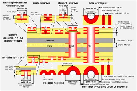
What is an HDI PCB Stackup?
An HDI PCB stackup refers to the arrangement of conductive layers, dielectric materials, and vias within a printed circuit board. The stackup determines the electrical characteristics, signal integrity, and mechanical properties of the PCB. In HDI PCBs, the stackup typically involves thinner dielectric layers, smaller vias, and more complex routing compared to traditional PCBs.

Types of HDI PCB Stackups
There are several types of HDI PCB stackups, each with its own advantages and limitations. Let’s explore the most common types:
1. Microvia Stackup
Microvia stackups are the most widely used type of HDI PCB stackup. They utilize small, laser-drilled vias with diameters typically ranging from 50 to 150 microns. These vias connect the outer layers to the inner layers of the PCB, enabling high-density routing and component placement.
Advantages:
– Allows for high component density and miniaturization
– Enables efficient use of board space
– Provides good signal integrity and reduced crosstalk
Limitations:
– Higher manufacturing costs compared to traditional PCBs
– Requires specialized equipment and processes for fabrication
2. Buried Via Stackup
Buried via stackups involve placing vias within the inner layers of the PCB, rather than connecting the outer layers to the inner layers. This type of stackup is useful when there is limited space on the outer layers or when additional shielding is required between layers.
Advantages:
– Provides better signal integrity and reduced crosstalk
– Allows for more efficient use of board space
– Enables the creation of isolated power and ground planes
Limitations:
– Higher manufacturing costs due to additional processing steps
– Increased complexity in design and fabrication
3. Staggered Via Stackup
Staggered via stackups use a combination of microvias and buried vias to create a more complex interconnect structure. In this type of stackup, the vias are placed in a staggered pattern, allowing for higher routing density and improved signal integrity.
Advantages:
– Enables high-density routing and component placement
– Provides excellent signal integrity and reduced crosstalk
– Allows for more design flexibility and optimization
Limitations:
– Higher manufacturing costs due to the complexity of the stackup
– Requires careful design and planning to ensure manufacturability
4. Any Layer Via Stackup
Any layer via stackups allow for the placement of vias on any layer of the PCB, providing the highest level of design flexibility. This type of stackup is often used in highly complex designs where routing density and signal integrity are critical.
Advantages:
– Provides the highest level of design flexibility and optimization
– Enables high-density routing and component placement
– Offers excellent signal integrity and reduced crosstalk
Limitations:
– Highest manufacturing costs among HDI PCB stackups
– Requires advanced design skills and specialized fabrication processes

Choosing the Right HDI PCB Stackup
When selecting the appropriate HDI PCB stackup for your design, consider the following factors:
-
Design Complexity: Evaluate the complexity of your design, including the number of components, routing density, and signal integrity requirements. More complex designs may require more advanced stackup types, such as staggered or any layer via stackups.
-
Manufacturing Cost: Consider the manufacturing costs associated with each stackup type. Microvia stackups are generally the most cost-effective, while buried via, staggered via, and any layer via stackups involve higher costs due to additional processing steps and complexity.
-
Board Size and Layer Count: The size of your PCB and the number of layers required will influence the choice of stackup. Smaller boards with fewer layers may benefit from microvia or buried via stackups, while larger and more complex boards may require staggered or any layer via stackups.
-
Signal Integrity Requirements: Assess the signal integrity requirements of your design, including the need for controlled impedance, reduced crosstalk, and shielding. Buried via and staggered via stackups offer better signal integrity compared to microvia stackups.
-
Manufacturing Capabilities: Consider the manufacturing capabilities of your chosen PCB fabrication partner. Some stackup types may require specialized equipment and processes that not all manufacturers can accommodate.

HDI PCB Stackup Comparison
To help you make an informed decision, here’s a comparison table of the different HDI PCB stackup types:
| Stackup Type | Advantages | Limitations | Typical Applications |
|---|---|---|---|
| Microvia | – High component density – Efficient board space use – Good signal integrity |
– Higher cost than traditional PCBs – Requires specialized equipment |
– Smartphones – Wearable devices – Internet of Things (IoT) devices |
| Buried Via | – Better signal integrity – Efficient board space use – Isolated power and ground planes |
– Higher cost due to additional processing – Increased design complexity |
– High-speed digital devices – RF and microwave applications – Automotive electronics |
| Staggered Via | – High routing density – Excellent signal integrity – Design flexibility |
– Higher cost due to stackup complexity – Requires careful design planning |
– High-performance computing – Telecommunications equipment – Medical devices |
| Any Layer Via | – Highest design flexibility – High routing density – Excellent signal integrity |
– Highest manufacturing cost – Requires advanced design skills |
– Aerospace and defense applications – High-end consumer electronics – Cutting-edge research and development |
Frequently Asked Questions (FAQ)
- What is the main difference between HDI PCBs and traditional PCBs?
-
HDI PCBs have smaller vias, thinner dielectric layers, and more complex routing compared to traditional PCBs, enabling higher component density and miniaturization.
-
Can I use a microvia stackup for a high-speed digital design?
-
While microvia stackups offer good signal integrity, buried via or staggered via stackups may be more suitable for high-speed digital designs due to their better signal integrity and reduced crosstalk.
-
How do I determine the appropriate layer count for my HDI PCB?
-
The layer count depends on the complexity of your design, routing requirements, and component placement. Work with your PCB design team and fabrication partner to determine the optimal layer count for your specific application.
-
Are HDI PCBs more expensive than traditional PCBs?
-
Yes, HDI PCBs generally have higher manufacturing costs compared to traditional PCBs due to the specialized equipment, processes, and materials required for their fabrication.
-
What should I consider when choosing a PCB fabrication partner for my HDI design?
- When selecting a PCB fabrication partner, consider their experience with HDI PCBs, available manufacturing capabilities, quality control processes, and ability to meet your specific design requirements and timeline.
Conclusion
Choosing the right HDI PCB stackup is essential for achieving optimal performance, manufacturability, and cost-effectiveness in your PCB design. By understanding the different types of stackups and their advantages and limitations, you can make an informed decision based on your specific design requirements.
When in doubt, consult with your PCB design team and fabrication partner to determine the best stackup for your application. With careful planning and execution, HDI PCBs can help you push the boundaries of innovation and create cutting-edge electronic devices.