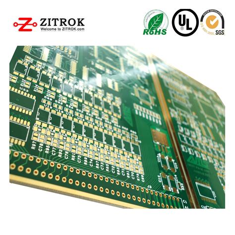
What is an HDI PCB?
HDI (High Density Interconnect) PCBs are printed circuit boards with a higher wiring density per unit area than conventional PCBs. This is achieved by incorporating thinner traces, smaller vias, and capture pads, and by using high-performance laminate materials.
HDI technology allows for denser component placement and more compact designs, enabling miniaturization of electronic devices. Some of the key characteristics of HDI PCBs include:
- Trace widths and spaces less than 100 μm (4 mil)
- Micro vias with diameters less than 150 μm (6 mil)
- Pad diameters less than 400 μm (16 mil)
- Thin copper foils and high-performance laminates
Benefits of HDI PCBs
HDI PCBs offer several advantages over traditional PCB designs:
-
Space Savings: The compact nature of HDI PCBs allows for smaller form factors and higher component density, making them ideal for portable and handheld devices.
-
Improved Signal Integrity: Shorter signal paths and reduced layer count in HDI designs lead to improved signal integrity and reduced electromagnetic interference (EMI).
-
Enhanced Thermal Management: HDI PCBs can dissipate heat more efficiently due to the presence of microvias and buried vias, which act as thermal conduits.
-
Cost Reduction: Although the initial setup costs for HDI PCBs may be higher, the overall cost can be lower due to reduced board size and layer count.

HDI PCB Design Considerations
When designing HDI PCBs, several factors must be taken into account to ensure optimal performance and manufacturability:
1. Layer Stack-up
The layer stack-up is a critical aspect of HDI PCB design. It determines the number of layers, their arrangement, and the interconnections between them. A typical HDI PCB Stack-up may include:
- Signal layers
- Ground and power planes
- Microvia layers
- Buried and blind vias
The choice of materials, layer thickness, and copper weights should be based on the specific requirements of the application, such as signal speed, impedance control, and thermal management.
2. Via Types and Sizes
HDI PCBs make use of various types of vias, each serving a specific purpose:
- Through Vias: These are the most common type of vias, extending through all layers of the PCB.
- Blind Vias: These vias are visible only on one side of the board and terminate at an inner layer.
- Buried Vias: These vias are used to interconnect inner layers and are not visible on either side of the board.
- Microvias: These are small, laser-drilled vias with diameters less than 150 μm, used for high-density interconnects.
The choice of via type and size depends on the design requirements, such as routing density, signal integrity, and manufacturability.
3. Trace Width and Spacing
HDI PCBs feature fine-pitch traces, with widths and spaces typically less than 100 μm (4 mil). The actual values depend on the PCB manufacturer’s capabilities and the specific design requirements.
When designing traces for HDI PCBs, consider the following:
- Current-carrying capacity
- Impedance control
- Signal integrity
- Manufacturability
Consult with your PCB manufacturer to determine the minimum trace width and spacing that can be reliably achieved.
4. Pad Size and Solder Mask Opening
Component pads on HDI PCBs are smaller than those on conventional PCBs, with diameters typically less than 400 μm (16 mil). The solder mask opening (SMO) should be designed to provide adequate clearance for the solder joint while preventing solder bridging.
The pad size and SMO depend on factors such as:
- Component package type
- Solder paste stencil thickness
- Solder joint reliability requirements
Work closely with your PCB manufacturer and assembly house to ensure the pad design is optimized for the specific manufacturing process.

HDI PCB Manufacturing Process
The manufacturing process for HDI PCBs involves several specialized techniques and technologies:
1. Material Selection
HDI PCBs require high-performance laminate materials that offer:
- Low dielectric constant and loss tangent
- High thermal stability
- Excellent mechanical properties
- Compatibility with fine-pitch fabrication processes
Some common materials used for HDI PCBs include:
- FR-4
- Polyimide
- PTFE (Teflon)
- BT-epoxy
- Ceramic
The choice of material depends on the specific application requirements, such as signal speed, thermal management, and cost.
2. Laser Drilling
Microvias in HDI PCBs are typically created using laser drilling. This process involves using a focused laser beam to create small, precise holes in the PCB substrate.
There are two main types of laser drilling:
- UV laser drilling: This method uses ultraviolet laser light to create vias with diameters as small as 25 μm.
- CO2 laser drilling: This method uses infrared laser light and is suitable for creating vias with diameters greater than 50 μm.
The choice of laser drilling method depends on the via size requirements and the capabilities of the PCB manufacturer.
3. Copper Plating
After the microvias are drilled, they are filled with copper to create electrical connections between layers. This is typically done using electroless and electrolytic copper plating processes.
The plating process involves the following steps:
- Cleaning and conditioning the via walls
- Applying a seed layer of copper using electroless plating
- Building up the copper thickness using electrolytic plating
The plating process must be carefully controlled to ensure uniform coverage and avoid voids or other defects.
4. Patterning and Etching
Once the copper plating is complete, the circuit pattern is created using photolithography and etching processes. This involves:
- Applying a photoresist layer to the copper surface
- Exposing the photoresist to UV light through a patterned mask
- Developing the photoresist to remove the unexposed areas
- Etching away the unwanted copper using a chemical etchant
- Stripping the remaining photoresist
The patterning and etching process must be optimized to achieve the fine feature sizes required for HDI PCBs.

HDI PCB Testing and Inspection
To ensure the quality and reliability of HDI PCBs, rigorous testing and inspection procedures are necessary. Some common methods include:
1. Automated Optical Inspection (AOI)
AOI uses high-resolution cameras and image processing software to detect surface defects such as:
- Broken traces
- Short circuits
- Solder bridges
- Missing components
AOI is a fast and efficient method for detecting visible defects, but it cannot identify internal issues.
2. X-Ray Inspection
X-ray inspection is used to detect internal defects in HDI PCBs, such as:
- Voids in vias and solder joints
- Misaligned or tilted components
- Insufficient solder fill
X-ray inspection provides a non-destructive means of evaluating the internal structure of the PCB.
3. Electrical Testing
Electrical testing is used to verify the functionality and performance of the HDI PCB. This may include:
- Continuity testing
- Insulation resistance testing
- High-potential (hipot) testing
- Impedance testing
Electrical testing helps to ensure that the PCB meets the specified electrical requirements and is free from shorts, opens, or other faults.
FAQ
1. What is the minimum feature size achievable with HDI PCBs?
The minimum feature size depends on the specific capabilities of the PCB manufacturer. Typically, HDI PCBs can achieve trace widths and spaces less than 100 μm (4 mil), microvia diameters less than 150 μm (6 mil), and pad diameters less than 400 μm (16 mil).
2. Are HDI PCBs more expensive than traditional PCBs?
The initial setup costs for HDI PCBs may be higher due to the specialized equipment and processes required. However, the overall cost can be lower due to the reduced board size and layer count, which leads to material and assembly cost savings.
3. What are the main applications for HDI PCBs?
HDI PCBs are commonly used in applications that require high component density, miniaturization, and improved signal integrity. Some examples include:
- Smartphones and tablets
- Wearable electronics
- Medical devices
- Aerospace and defense systems
- High-speed networking equipment
4. Can HDI PCBs be used for high-power applications?
While HDI PCBs are primarily designed for high-speed and high-density applications, they can be used for high-power applications with proper design considerations. This may involve the use of thicker copper layers, specialized materials, and enhanced thermal management techniques.
5. How can I ensure the manufacturability of my HDI PCB design?
To ensure the manufacturability of your HDI PCB design, follow these best practices:
- Consult with your PCB manufacturer early in the design process
- Adhere to the manufacturer’s design guidelines for minimum feature sizes and clearances
- Use standard via sizes and pad shapes whenever possible
- Perform thorough design rule checks (DRC) and manufacturability audits
- Provide clear and accurate documentation, including Gerber files, drill files, and assembly drawings
By working closely with your PCB manufacturer and following industry best practices, you can achieve a perfect HDI PCB design that meets your performance, reliability, and cost requirements.