Judy@4pcba.com
7:30 AM - 7:30 PM
Monday to Saturday

Archive: April 3, 2024

What items can be reverse-engineered?

Consumer Electronics

One of the most popular categories of items to reverse engineer is consumer electronics. This includes devices like smartphones, tablets, laptops, smart home gadgets, and wearable technology. By disassembling these products and examining their internal components and circuitry, engineers and hobbyists can gain valuable insights into how they work.

Some reasons to reverse engineer consumer electronics include:
– Understanding the underlying technology and design principles
– Identifying potential security vulnerabilities or exploits
– Developing compatible accessories, peripherals, or software
– Creating clones or knockoff versions of popular products
– Repairing or modifying devices for custom applications

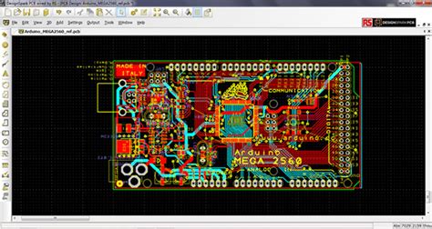
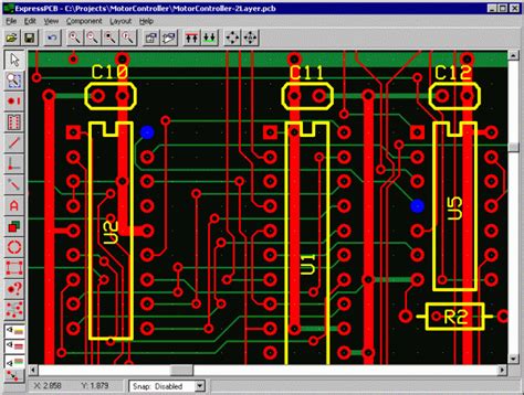
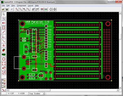
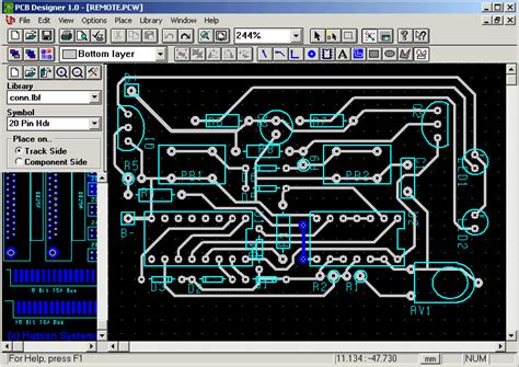
The process of Reverse Engineering consumer electronics typically involves several steps:

  1. Disassembly – Carefully taking apart the device to access its internal components
  2. Documentation – Taking photos and notes on the layout, components, and connections
  3. Schematic Capture – Creating a detailed diagram of the circuitry and components
  4. Analysis – Examining the components and circuitry to understand their functions
  5. Prototyping – Building a working replica or modified version of the device
  6. Testing & Refinement – Testing the prototype to ensure it functions properly and making any necessary adjustments

Some examples of consumer electronics that are frequently reverse-engineered include:

Device Reason for Reverse Engineering
iPhone Creating unofficial repair guides, developing 3rd-party accessories
Fitbit Analyzing fitness tracking algorithms, building custom apps
Nest Thermostat Integrating with home automation systems, improving energy efficiency
Bluetooth Headphones Developing compatible audio codecs, enhancing sound quality

While reverse engineering consumer electronics can be a challenging and time-consuming process, it offers valuable opportunities for learning, innovation, and customization. However, it’s important to be aware of any legal or intellectual property considerations, as some companies may object to their products being reverse-engineered or modified.

Mechanical Devices

Another common category of Reverse-engineerable items is mechanical devices. This includes everything from simple tools and appliances to complex machinery and vehicles. By disassembling and analyzing these devices, engineers can learn how they work and identify opportunities for improvement or customization.

Some reasons to reverse engineer mechanical devices include:
– Understanding the design principles and mechanical systems involved
– Identifying potential failure points or maintenance requirements
– Developing compatible replacement parts or accessories
– Creating custom modifications or adaptations for specific applications
– Improving performance, efficiency, or durability

The process of reverse engineering mechanical devices is similar to that of consumer electronics, but with a greater emphasis on physical components and mechanisms:

  1. Disassembly – Taking apart the device to access its internal components and mechanisms
  2. Documentation – Taking photos and measurements of each component and assembly
  3. 3D Modeling – Creating detailed CAD models of the components and assemblies
  4. Analysis – Examining the mechanical systems and identifying their functions and interactions
  5. Prototyping – Fabricating replica or modified components, often using 3D printing or CNC machining
  6. Testing & Refinement – Assembling the prototype and testing it to ensure proper function and fitment

Some examples of mechanical devices that are often reverse-engineered include:

Device Reason for Reverse Engineering
Automotive Components Developing aftermarket replacement parts, improving performance
Industrial Machinery Creating custom tooling or automation systems, increasing efficiency
Medical Devices Analyzing mechanisms and materials, ensuring safety and reliability
Aerospace Components Optimizing strength-to-weight ratios, improving fuel efficiency

Reverse engineering mechanical devices requires a solid understanding of mechanical principles, materials science, and manufacturing processes. It also often involves the use of specialized tools and equipment, such as 3D scanners, CAD software, and CNC machines.

Software and Firmware

In addition to physical products, software and firmware are also common targets for reverse engineering. This involves analyzing the code and logic of a program to understand how it works and identify potential vulnerabilities or opportunities for modification.

Some reasons to reverse engineer software and firmware include:
– Understanding the algorithms and logic used in the program
– Identifying security vulnerabilities or exploits
– Developing compatible plugins, extensions, or integrations
– Creating interoperability between different systems or platforms
– Modifying or customizing the behavior of the software

The process of reverse engineering software and firmware typically involves several steps:

  1. Decompilation – Converting the compiled binary code back into a human-readable format
  2. Analysis – Examining the decompiled code to understand its structure, functions, and logic
  3. Debugging – Using debuggers and other tools to step through the code and observe its behavior
  4. Modification – Making changes to the code to alter its functionality or add new features
  5. Recompilation – Compiling the modified code back into a binary format
  6. Testing – Running the modified software to ensure it functions as intended

Some examples of software and firmware that are frequently reverse-engineered include:

Software Reason for Reverse Engineering
Operating Systems Developing custom drivers or kernels, analyzing security features
Embedded Firmware Customizing device behavior, adding new functionality
Proprietary Algorithms Understanding the underlying logic, developing compatible implementations
Legacy Software Migrating to modern platforms, ensuring compatibility with newer systems

Reverse engineering software and firmware requires strong programming skills and familiarity with a variety of tools and techniques, such as disassemblers, debuggers, and hex editors. It also often involves working with low-level languages like assembly and navigating complex code structures.

Conclusion

Reverse engineering is a powerful tool for understanding, replicating, and improving a wide range of products and systems. From consumer electronics and mechanical devices to software and firmware, almost anything can be reverse-engineered with the right skills, tools, and techniques.

While reverse engineering can be a challenging and time-consuming process, it offers valuable opportunities for learning, innovation, and customization. By analyzing how things work and identifying opportunities for improvement, reverse engineers can create new products, enhance existing ones, and push the boundaries of what’s possible.

However, it’s important to approach reverse engineering with caution and respect for intellectual property rights. Many companies invest significant resources into developing their products, and may object to having their designs copied or modified without permission. As such, it’s crucial to carefully consider the legal and ethical implications of reverse engineering before embarking on any projects.

Ultimately, the key to successful reverse engineering is a combination of technical skill, creative problem-solving, and a deep curiosity about how things work. Whether you’re a professional engineer, a hobbyist tinkerer, or just someone who likes to take things apart and see what makes them tick, reverse engineering offers endless opportunities for learning and discovery.

Frequently Asked Questions

Is reverse engineering legal?

The legality of reverse engineering depends on the specific circumstances and jurisdiction. In many cases, reverse engineering is protected under fair use doctrines or other legal provisions, especially if it’s done for the purposes of interoperability, education, or research. However, some companies may object to their products being reverse-engineered, especially if the results are used to create competing products or circumvent security measures. It’s important to carefully consider the legal implications of reverse engineering before proceeding with any projects.

What tools are used for reverse engineering?

The tools used for reverse engineering vary depending on the type of item being analyzed. For consumer electronics and mechanical devices, common tools include screwdrivers, pliers, multimeters, oscilloscopes, 3D scanners, and CAD software. For software and firmware, common tools include disassemblers, debuggers, hex editors, and decompilers.

How long does it take to reverse engineer something?

The time required to reverse engineer something depends on the complexity of the item, the skills and experience of the engineer, and the tools and resources available. Simple devices or programs may only take a few hours or days to reverse engineer, while more complex systems can take weeks, months, or even years. Reverse engineering is often an iterative process, with multiple rounds of analysis, prototyping, and testing required to fully understand and replicate the item.

What skills are needed for reverse engineering?

Reverse engineering requires a diverse set of skills, depending on the type of item being analyzed. For consumer electronics and mechanical devices, important skills include electrical and mechanical engineering, materials science, and manufacturing processes. For software and firmware, important skills include programming, software architecture, and familiarity with low-level languages like assembly. In general, successful reverse engineering also requires strong problem-solving skills, attention to detail, and the ability to think creatively and analytically.

Can I reverse engineer something and sell the results?

The answer to this question depends on the specific item being reverse-engineered and the applicable laws and regulations. In some cases, reverse engineering and selling the results may be protected under fair use or other legal doctrines, especially if the results are used for interoperability or other legitimate purposes. However, in other cases, selling reverse-engineered products may be considered copyright or patent infringement, especially if the original item is protected by intellectual property laws. It’s important to carefully consider the legal implications of reverse engineering and consult with qualified legal professionals before attempting to sell any reverse-engineered products.

What software to use for PCB?

Introduction to PCB Design Software

Printed Circuit Board (PCB) design is a crucial aspect of modern electronics. Choosing the right PCB software can greatly impact the efficiency and quality of your design process. In this article, we will explore various PCB software options, their features, and their suitability for different design requirements.

Types of PCB Design Software

1. EDA (Electronic Design Automation) Software

EDA software is the most comprehensive type of PCB design software. It offers a wide range of features and tools for designing, simulating, and analyzing PCBs. Some popular EDA software include:

  • Altium Designer
  • Cadence OrCAD
  • Mentor Graphics PADS
  • Zuken CR-8000

These software packages are suitable for complex designs and large-scale projects.

2. CAD (Computer-Aided Design) Software

CAD software is primarily used for creating 2D and 3D designs. While not specifically designed for PCBs, some CAD software have PCB design capabilities or extensions. Examples include:

  • AutoCAD
  • SolidWorks PCB
  • Fusion 360

CAD software is a good choice for mechanical designers who need to integrate PCB design into their workflow.

3. Open-Source PCB Software

Open-source PCB software is freely available and often community-driven. These software offer basic to advanced PCB design features and are suitable for hobbyists, students, and small-scale projects. Some popular open-source PCB software include:

  • KiCad
  • EAGLE (free version)
  • gEDA

While open-source software may lack some advanced features found in commercial software, they are constantly improving and can be a cost-effective solution.

Features to Consider When Choosing PCB Software

When selecting PCB software, consider the following features:

  1. Schematic Capture: The ability to create and edit schematic diagrams easily.
  2. PCB Layout: Tools for designing the physical layout of the PCB, including component placement, routing, and layer management.
  3. Library Management: Extensive component libraries and the ability to create and manage custom libraries.
  4. Simulation and Analysis: Tools for simulating and analyzing circuit behavior, signal integrity, and electromagnetic compatibility.
  5. Manufacturing Output: Support for generating manufacturing files, such as Gerber files, drill files, and bill of materials (BOM).
  6. Collaboration and Version Control: Features for collaborating with team members and managing design revisions.
  7. User Interface and Ease of Use: An intuitive user interface and helpful documentation or tutorials.
Feature EDA Software CAD Software Open-Source Software
Schematic Capture ✔️ ✔️ ✔️
PCB Layout ✔️ ✔️ ✔️
Library Management ✔️ ✔️ ✔️
Simulation and Analysis ✔️ Limited Limited
Manufacturing Output ✔️ ✔️ ✔️
Collaboration & Version Control ✔️ ✔️ Limited
User Interface & Ease of Use ✔️ ✔️ ✔️

Choosing the Right PCB Software for Your Needs

Hobbyists and Students

For hobbyists and students, open-source PCB software like KiCad or the free version of EAGLE is a great starting point. These software offer a good balance of features and ease of use, without the cost of commercial software.

Small to Medium-Sized Projects

For small to medium-sized projects, mid-range EDA software like EAGLE (paid version) or Altium CircuitMaker can be a good choice. These software offer more advanced features than open-source options, while still being relatively affordable.

Large-Scale and Complex Projects

For large-scale and complex projects, high-end EDA software like Altium Designer, Cadence OrCAD, or Mentor Graphics PADS are recommended. These software offer the most comprehensive set of features and tools for designing, simulating, and analyzing complex PCBs.

Mechanical Designers

For mechanical designers who need to integrate PCB design into their workflow, CAD software with PCB capabilities, such as SolidWorks PCB or Autodesk Fusion 360, can be a good choice. These software allow for seamless integration between mechanical and electronic design.

Popular PCB Software Comparison

Software Type Price Range Ease of Use Features
Altium Designer EDA High Moderate ✔️✔️✔️✔️
KiCad Open-Source Free Moderate ✔️✔️✔️
EAGLE EDA Low to Mid Easy ✔️✔️✔️
OrCAD EDA High Moderate ✔️✔️✔️✔️
Fusion 360 CAD Mid Easy ✔️✔️

Frequently Asked Questions (FAQ)

  1. Q: What is the best PCB software for beginners?
    A: For beginners, open-source software like KiCad or the free version of EAGLE is a good starting point. These software offer a good balance of features and ease of use, without the cost of commercial software.

  2. Q: Can I use CAD software for PCB design?
    A: Yes, some CAD software, such as SolidWorks PCB and Autodesk Fusion 360, have PCB design capabilities or extensions. These software are suitable for mechanical designers who need to integrate PCB design into their workflow.

  3. Q: What are the advantages of using EDA software for PCB design?
    A: EDA software offers the most comprehensive set of features and tools for designing, simulating, and analyzing PCBs. They are suitable for complex designs and large-scale projects, and offer advanced features like simulation and analysis, collaboration, and version control.

  4. Q: Are open-source PCB software reliable?
    A: Yes, open-source PCB software like KiCad and gEDA are reliable and constantly improving. They are community-driven and offer a cost-effective solution for hobbyists, students, and small-scale projects.

  5. Q: How do I choose the right PCB software for my needs?
    A: When choosing PCB software, consider your design requirements, budget, and skill level. Hobbyists and students may prefer open-source software, while large-scale and complex projects may require high-end EDA software. Mechanical designers may benefit from CAD software with PCB capabilities.

Conclusion

Choosing the right PCB software is essential for efficient and high-quality PCB design. Consider your design requirements, budget, and skill level when selecting PCB software. EDA software offers the most comprehensive features for complex designs, while open-source software is a cost-effective solution for hobbyists and small-scale projects. CAD software with PCB capabilities is suitable for mechanical designers who need to integrate PCB design into their workflow.

By understanding the different types of PCB software, their features, and their suitability for various design needs, you can make an informed decision and choose the best PCB software for your project.

Can you reverse engineer a PCB board?

What is PCB reverse engineering?

Reverse-Engineering/”>PCB reverse engineering is the process of examining an existing PCB to determine its design, components, and functionality. This process typically involves a combination of visual inspection, electrical testing, and software analysis. The goal is to create a detailed understanding of the PCB, which can be used for various purposes, such as:

  • Creating documentation for an undocumented PCB
  • Developing a compatible or clone product
  • Updating or improving an existing design
  • Analyzing and troubleshooting issues with a PCB
  • Learning from the design techniques used in the PCB

The process of reverse-engineering a PCB

The process of reverse-engineering a PCB can be broken down into several key steps:

  1. Visual inspection: The first step is to visually examine the PCB, taking note of its overall layout, components, and any identifying markings or labels. High-resolution images of both sides of the PCB are often captured for reference.

  2. Component identification: Each component on the PCB is identified and documented, including its type (resistor, capacitor, IC, etc.), value, and package. This information is used to create a bill of materials (BOM) for the PCB.

  3. Schematic capture: The electrical connections between components are traced and documented, creating a schematic diagram of the PCB. This process can be done manually or with the help of software tools.

  4. PCB layout: The physical layout of the PCB is captured, including the location and orientation of components, traces, and vias. This information is used to create a PCB layout file that can be used for manufacturing.

  5. Functional analysis: The functionality of the PCB is analyzed and documented, including its inputs, outputs, and any special features or functions. This may involve additional testing and reverse-engineering of the device’s firmware or software.

Tools for PCB reverse engineering

There are several tools and techniques that can be used to aid in the process of PCB reverse engineering:

  1. Microscopes and magnifiers: Visual inspection of a PCB often requires the use of microscopes or magnifiers to clearly see small components and traces.

  2. Multimeters and oscilloscopes: Electrical testing of a PCB may involve the use of multimeters to measure resistance, voltage, and continuity, as well as oscilloscopes to analyze signals and waveforms.

  3. Schematic capture software: Software tools like Eagle, KiCad, and Altium Designer can be used to create schematic diagrams from the information gathered during reverse engineering.

  4. PCB layout software: The same software tools used for schematic capture can also be used to create PCB layout files from the reverse-engineered data.

  5. Firmware and software analysis tools: If the PCB includes a microcontroller or other programmable device, additional tools may be needed to analyze and reverse-engineer its firmware or software.

Tool Purpose
Microscopes and magnifiers Visual inspection of small components and traces
Multimeters and oscilloscopes Electrical testing and signal analysis
Schematic capture software Creating schematic diagrams from reverse-engineered data
PCB layout software Creating PCB layout files from reverse-engineered data
Firmware and software analysis tools Analyzing and reverse-engineering firmware or software

Challenges in PCB reverse engineering

Reverse engineering a PCB can be a complex and time-consuming process, and there are several challenges that may be encountered:

  1. Component identification: Some components may be difficult to identify, especially if they are custom or proprietary parts. In some cases, the markings on a component may be obscured or missing entirely.

  2. Trace routing: Following the traces on a PCB can be challenging, particularly if the board has multiple layers or uses small traces and vias.

  3. Undocumented features: The PCB may include undocumented features or functions that are not immediately apparent from visual inspection or electrical testing.

  4. Legal considerations: In some cases, reverse engineering a PCB may be restricted by intellectual property laws or other legal considerations. It is important to ensure that any reverse engineering activities are conducted legally and ethically.

Best practices for PCB reverse engineering

To ensure successful and efficient PCB reverse engineering, consider the following best practices:

  1. Document everything: Thorough documentation is essential for successful reverse engineering. Take detailed notes, capture high-quality images, and create clear schematic diagrams and PCB layouts.

  2. Work methodically: Follow a systematic approach to reverse engineering, starting with visual inspection and component identification before moving on to more complex tasks like schematic capture and functional analysis.

  3. Use appropriate tools: Invest in high-quality tools and software to aid in the reverse engineering process, such as microscopes, multimeters, and schematic capture software.

  4. Collaborate with others: PCB reverse engineering can be a complex and time-consuming process, so it can be helpful to collaborate with others who have experience or expertise in this area.

  5. Respect intellectual property: Always ensure that any reverse engineering activities are conducted legally and ethically, respecting the intellectual property rights of the original designers and manufacturers.

FAQ

  1. Is PCB reverse engineering legal?
    PCB reverse engineering is legal in many cases, particularly if the purpose is for learning, research, or compatibility. However, it is important to ensure that any reverse engineering activities do not violate intellectual property laws or other legal restrictions.

  2. How long does it take to reverse engineer a PCB?
    The time required to reverse engineer a PCB can vary widely depending on the complexity of the board, the tools and techniques used, and the experience of the person conducting the reverse engineering. Simple PCBs may take a few hours, while more complex boards could take weeks or even months.

  3. What skills are needed for PCB reverse engineering?
    PCB reverse engineering requires a combination of skills, including knowledge of electronics, experience with PCB design and manufacturing, familiarity with schematic capture and PCB layout software, and strong problem-solving and analytical skills.

  4. Can I use reverse-engineered PCB designs for commercial purposes?
    Using reverse-engineered PCB designs for commercial purposes may be restricted by intellectual property laws or other legal considerations. It is important to carefully review any applicable laws and regulations before using reverse-engineered designs for commercial purposes.

  5. What are the benefits of PCB reverse engineering?
    PCB reverse engineering can provide several benefits, such as understanding how a device works, creating compatible or clone products, updating or improving existing designs, analyzing and troubleshooting issues, and learning from the design techniques used in the original PCB.

Conclusion

Reverse engineering a PCB can be a complex and challenging process, but it is also a valuable skill for anyone working with electronics. By following a systematic approach, using appropriate tools and techniques, and collaborating with others, it is possible to successfully reverse engineer a PCB and gain a detailed understanding of its design and functionality. However, it is important to always conduct reverse engineering activities legally and ethically, respecting the intellectual property rights of the original designers and manufacturers.

How to do reverse engineering of PCB board?

Understanding PCB Reverse Engineering

Printed Circuit Board (PCB) reverse engineering is the process of analyzing and understanding the design and functionality of an existing PCB. It involves examining the board’s layout, components, and connections to create a schematic diagram or recreate the original design files. Reverse-Engineering/”>PCB Reverse Engineering is useful in various scenarios, such as:

  • Repairing or modifying an old or damaged PCB
  • Understanding the functionality of a PCB when documentation is unavailable
  • Identifying potential design flaws or improvements
  • Competitive analysis and product benchmarking

Key Steps in PCB Reverse Engineering

  1. Visual inspection and documentation
  2. Component identification
  3. Tracing connections and creating a schematic
  4. Recreating PCB layout
  5. Verification and testing

Visual Inspection and Documentation

The first step in PCB reverse engineering is to thoroughly inspect the board and document its physical characteristics. This includes:

Board Dimensions and Layer Count

Measure the length, width, and thickness of the PCB. Determine the number of layers by examining the edge of the board or using a microscope to count the copper layers.

Component Placement and Orientation

Note the location and orientation of each component on the board. Take high-resolution photographs of both sides of the PCB for reference.

Connectors and Input/Output (I/O) Interfaces

Identify the types of connectors used (e.g., USB, HDMI, power) and their pinouts. Document any other I/O interfaces, such as buttons, switches, or displays.

Component Identification

Identifying the components on the PCB is crucial for understanding its functionality and creating an accurate schematic.

Integrated Circuits (ICs)

Identify ICs by their markings or package types. Use datasheets and reference guides to determine their functions and pinouts.

Passive Components

Identify resistors, capacitors, and inductors by their markings, color codes, or package sizes. Measure their values using a multimeter if necessary.

Other Components

Identify other components, such as diodes, transistors, crystals, and connectors, based on their markings and package types.

Tracing Connections and Creating a Schematic

Once the components are identified, trace the connections between them to create a schematic diagram.

Continuity Testing

Use a multimeter to test for continuity between component pins and PCB traces. This helps determine which pins are connected.

Visual Tracing

Follow the PCB traces visually to identify connections between components. Use a magnifying glass or microscope for small or dense boards.

Schematic Capture Software

Use schematic capture software, such as KiCad or Eagle, to create a digital schematic based on the traced connections. Assign component symbols and values based on the identified components.

Recreating PCB Layout

After creating the schematic, recreate the PCB layout using PCB design software.

PCB Design Software

Use PCB design software, such as KiCad or Eagle, to create a new PCB layout based on the schematic and the original board’s dimensions.

Component Placement

Place components on the recreated PCB layout in the same locations and orientations as the original board.

Routing

Route the connections between components based on the original PCB’s trace patterns. Use the same or similar trace widths and clearances.

Verification and Testing

Once the schematic and PCB layout are recreated, verify their accuracy and test the functionality of the reverse-engineered design.

Design Rule Check (DRC)

Run a DRC on the recreated PCB layout to ensure it meets manufacturing requirements and design guidelines.

Prototype Fabrication

Fabricate a prototype of the reverse-engineered PCB using the recreated design files.

Functional Testing

Test the prototype to verify that it functions identically to the original PCB. Compare the prototype’s performance, power consumption, and signal integrity to the original board.

Tools and Equipment for PCB Reverse Engineering

To effectively perform PCB reverse engineering, you’ll need the following tools and equipment:

Tool/Equipment Purpose
Digital multimeter Testing continuity, measuring component values
Oscilloscope Analyzing signals and waveforms
Logic analyzer Capturing and analyzing digital signals
Microscope Examining small components and PCB traces
Soldering iron and desoldering tools Removing and replacing components
Schematic capture software Creating digital schematics
PCB design software Recreating PCB layouts
High-resolution camera Documenting the original PCB

Challenges in PCB Reverse Engineering

PCB reverse engineering can be a complex and time-consuming process, with several challenges to overcome:

Multilayer Boards

Reverse engineering multilayer PCBs is more difficult than single-layer boards, as traces can be hidden between layers. Special techniques, such as X-ray imaging or layer-by-layer deconstruction, may be required.

Damaged or Corroded Boards

Boards that are damaged or have corroded traces can be challenging to reverse engineer. Careful cleaning and repair may be necessary before the reverse engineering process can begin.

Obsolete or Custom Components

Some PCBs may contain obsolete or custom components that are difficult to identify or source. In such cases, finding a suitable replacement or understanding the component’s functionality can be challenging.

Intellectual Property and Legal Considerations

Reverse engineering a PCB may raise intellectual property and legal concerns, especially if the board is protected by patents or trade secrets. It’s essential to ensure that reverse engineering is performed for legitimate purposes and does not infringe on the rights of others.

FAQ

  1. Q: How long does it take to reverse engineer a PCB?
    A: The time required to reverse engineer a PCB depends on factors such as the board’s complexity, size, and the engineer’s experience. Simple boards may take a few hours, while complex, multilayer boards can take several days or weeks.

  2. Q: Can I reverse engineer a PCB without the original design files?
    A: Yes, it’s possible to reverse engineer a PCB without the original design files. However, the process will be more challenging and time-consuming, as you’ll need to manually trace connections and identify components.

  3. Q: Is it legal to reverse engineer a PCB?
    A: The legality of reverse engineering a PCB depends on the specific circumstances and the laws of your jurisdiction. In general, reverse engineering for the purpose of interoperability, repair, or academic study is permitted under fair use. However, reverse engineering for the purpose of copying or infringing on intellectual property rights may be illegal.

  4. Q: Can I use the reverse-engineered PCB design for commercial purposes?
    A: The ability to use a reverse-engineered PCB design for commercial purposes depends on the original design’s intellectual property protection and the laws of your jurisdiction. If the original design is protected by patents or copyrights, using the reverse-engineered design for commercial purposes without permission may be illegal.

  5. Q: What skills are required for PCB reverse engineering?
    A: PCB reverse engineering requires a combination of skills, including:

  6. Knowledge of electronic components and their functions
  7. Understanding of PCB design principles and manufacturing processes
  8. Proficiency in using schematic capture and PCB design software
  9. Experience with electronic test and measurement equipment
  10. Attention to detail and problem-solving skills

Conclusion

PCB reverse engineering is a valuable skill for anyone working with electronic hardware, enabling the understanding, repair, and modification of existing PCBs. By following the steps outlined in this article and using the appropriate tools and equipment, you can successfully reverse engineer a PCB and recreate its schematic and layout.

However, it’s essential to approach PCB reverse engineering with caution, taking into account the potential challenges and legal considerations involved. With practice and experience, you can develop the skills necessary to effectively reverse engineer PCBs and unlock the secrets of electronic hardware design.

What items are used for reverse engineering?

Table of Contents

Hardware Tools for Reverse Engineering

Screwdrivers and Pliers

Screwdrivers and pliers are essential tools for disassembling and reassembling hardware components. A variety of screwdriver types, such as flathead, Phillips, and Torx, are necessary to handle different screw sizes and heads. Pliers, including needle-nose and adjustable pliers, are useful for gripping and manipulating small components.

Soldering Iron and Desoldering Tools

A soldering iron is used to join electronic components and create electrical connections. When reverse engineering hardware, a soldering iron may be necessary to modify or repair circuitry. Desoldering tools, such as desoldering pumps and desoldering wicks, are used to remove solder and components from printed circuit boards (PCBs).

Multimeter

A multimeter is an electronic measuring instrument that combines several measurement functions, including voltage, current, and resistance. It is an essential tool for analyzing and troubleshooting electronic circuits during the reverse engineering process. Multimeters help identify faulty components, trace signals, and verify connections.

Oscilloscope

An oscilloscope is a device that graphically displays electrical signals and their changes over time. It is particularly useful for analyzing analog circuits and identifying signal patterns. Oscilloscopes are valuable for reverse engineering complex electronic systems, such as communication devices and control systems.

Logic Analyzer

A logic analyzer is a tool used to capture and display multiple digital signals simultaneously. It helps in understanding the behavior and timing of digital circuits. Logic analyzers are particularly useful for reverse engineering digital systems, such as microcontrollers and field-programmable gate arrays (FPGAs).

Software Tools for Reverse Engineering

Disassemblers and Decompilers

Disassemblers and decompilers are software tools used to analyze and understand the assembly code and source code of a program, respectively. Disassemblers convert machine code into human-readable assembly language, while decompilers attempt to recreate the original high-level source code from the machine code. These tools are essential for reverse engineering software, as they help in understanding the program’s structure, functionality, and potential vulnerabilities.

Tool Description Platform
IDA Pro Powerful disassembler and debugger Windows, Linux, macOS
Ghidra Open-source software Reverse Engineering Tool Windows, Linux, macOS
Hopper Reverse engineering tool for macOS and Linux macOS, Linux
Binary Ninja Reverse engineering platform with API support Windows, Linux, macOS

Debuggers

Debuggers are software tools that allow developers to examine and control the execution of a program. They are used to step through code, set breakpoints, inspect variables, and analyze program behavior. Debuggers are valuable for reverse engineering, as they help in understanding the program’s flow and identifying critical points of interest.

Tool Description Platform
GDB GNU Debugger, a powerful command-line debugger Windows, Linux, macOS
OllyDbg x86 debugger for Windows Windows
WinDbg Microsoft’s debugger for Windows Windows
LLDB Debugger for the LLVM project Windows, Linux, macOS

Hex Editors

Hex editors are software tools that allow users to view and edit the raw hexadecimal representation of a file. They are useful for analyzing binary data, identifying file signatures, and modifying binary files. Hex editors are often used in reverse engineering to examine and manipulate firmware, file formats, and network packets.

Tool Description Platform
HxD Freeware hex editor with disk editor capabilities Windows
010 Editor Professional text and hex editor Windows, Linux, macOS
WinHex Hex editor with data recovery and analysis features Windows
Hex Fiend Open-source hex editor for macOS macOS

Network Analysis Tools

Network analysis tools are used to capture, analyze, and interpret network traffic. They are valuable for reverse engineering network protocols, understanding communication patterns, and identifying security vulnerabilities. Network analysis tools help in decoding packet structures, extracting data, and reconstructing network conversations.

Tool Description Platform
Wireshark Powerful network protocol analyzer Windows, Linux, macOS
Tcpdump Command-line network packet analyzer Linux, macOS
Fiddler Web debugging proxy for analyzing HTTP/HTTPS traffic Windows, macOS, Linux
Nmap Network exploration and security auditing tool Windows, Linux, macOS

Imaging and Documentation Tools

Cameras and Microscopes

Cameras and microscopes are used to capture high-resolution images of hardware components, PCBs, and other physical objects. These images serve as visual references during the reverse engineering process and help in documenting the findings. High-quality images can reveal intricate details, such as component markings, circuit traces, and manufacturing defects.

Scanners and Photocopiers

Scanners and photocopiers are used to digitize technical documents, schematics, and manuals related to the product being reverse engineered. Having digital copies of these materials allows for easy sharing, annotation, and analysis. Scanned documents can be processed using optical character recognition (OCR) software to extract text and enable searching.

Diagramming Software

Diagramming software is used to create visual representations of the reverse-engineered system, such as flowcharts, circuit diagrams, and block diagrams. These diagrams help in understanding the system’s architecture, data flow, and functional relationships. Popular diagramming tools include Microsoft Visio, Draw.io, and Lucidchart.

Protection and Safety Equipment

Anti-static Wrist Strap

An anti-static wrist strap is a safety device used to prevent electrostatic discharge (ESD) damage to sensitive electronic components. When working with PCBs and other electronic devices during reverse engineering, wearing an anti-static wrist strap helps dissipate static charges and protects the components from potential damage.

Safety Glasses and Gloves

Safety glasses and gloves are essential personal protective equipment (PPE) when working with hardware components. Safety glasses protect the eyes from debris, splinters, and other hazards that may arise during disassembly or soldering. Gloves, such as nitrile or latex gloves, protect the hands from cuts, burns, and chemical exposure.

Frequently Asked Questions (FAQ)

What is the most essential tool for hardware reverse engineering?

The most essential tool for hardware reverse engineering is a good set of screwdrivers and pliers. These tools are necessary for disassembling and reassembling hardware components, which is a crucial step in the reverse engineering process. Without the ability to access the internal components, further analysis and understanding of the system would be limited.

Can I use free software tools for reverse engineering?

Yes, there are several free and open-source software tools available for reverse engineering. Examples include Ghidra, a powerful software reverse engineering tool developed by the National Security Agency (NSA), and GDB, a widely used debugger. These tools offer a range of features and capabilities that can be used effectively in reverse engineering projects.

Is reverse engineering legal?

The legality of reverse engineering depends on the specific circumstances and applicable laws. In many cases, reverse engineering is legal when done for the purpose of interoperability, research, or educational purposes. However, reverse engineering may be illegal if it involves circumventing copy protection, violating intellectual property rights, or breaching contractual agreements. It is important to consult with legal experts and understand the relevant laws before engaging in reverse engineering activities.

What skills are required for effective reverse engineering?

Effective reverse engineering requires a combination of technical skills and analytical abilities. Some of the key skills include:
– Programming and scripting: Proficiency in languages such as C, C++, Python, and assembly is beneficial for understanding and analyzing code.
– Electronics and hardware knowledge: Understanding of electronic components, circuits, and hardware architectures is crucial for reverse engineering physical systems.
– Problem-solving and critical thinking: The ability to break down complex systems, identify patterns, and develop logical conclusions is essential.
– Attention to detail: Reverse engineering often involves analyzing intricate details and subtle nuances, requiring a keen eye and meticulous approach.
– Patience and persistence: Reverse engineering can be a time-consuming and challenging process, requiring patience and persistence to overcome obstacles and uncover insights.

How long does it take to reverse engineer a product?

The time required to reverse engineer a product varies significantly depending on the complexity of the system, the available resources, and the desired level of understanding. Simple products or components may take a few hours or days to reverse engineer, while complex systems, such as advanced software applications or sophisticated hardware devices, can take weeks, months, or even years. The time invested in reverse engineering also depends on the individual’s skills, experience, and the specific goals of the project.

In conclusion, reverse engineering is a complex and multifaceted process that requires a variety of tools and equipment. From hardware tools like screwdrivers and multimeters to software tools like disassemblers and debuggers, each item plays a crucial role in analyzing and understanding the target system. Imaging and documentation tools help in capturing and organizing the findings, while protection and safety equipment ensure the well-being of both the reverse engineer and the components being examined.

Effective reverse engineering demands a combination of technical skills, analytical thinking, and perseverance. It is essential to understand the legal implications and ethical considerations associated with reverse engineering and to proceed with caution and responsibility.

By leveraging the appropriate tools and techniques, reverse engineering can provide valuable insights, enable interoperability, and drive innovation across various domains, including software development, hardware design, and security research. As technology continues to evolve, the importance of reverse engineering will only grow, making it an indispensable skill for professionals in the field.

Can a PCB be reverse engineered?

What is PCB Reverse Engineering?

Reverse-Engineering/”>PCB Reverse Engineering is the process of analyzing a printed circuit board to understand its design, functionality, and components without having access to the original design files or documentation. This process involves a combination of visual inspection, electrical testing, and software analysis to create a detailed representation of the PCB’s layout, components, and connections.

There are several reasons why someone might need to reverse engineer a PCB:

  1. Legacy systems: When dealing with older electronic devices for which documentation is no longer available, reverse engineering can help understand the PCB’s design and functionality.

  2. Competitive analysis: Companies may reverse engineer a competitor’s product to understand its inner workings and identify potential improvements or vulnerabilities.

  3. Failure analysis: When a PCB fails, reverse engineering can help identify the root cause of the failure and develop a solution.

  4. Intellectual property disputes: In cases where there are concerns about intellectual property infringement, reverse engineering can provide evidence to support or refute these claims.

The PCB reverse engineering process

The PCB reverse engineering process typically involves several steps, each requiring specific tools and expertise. Here’s a breakdown of the main stages:

1. Visual inspection

The first step in PCB reverse engineering is to visually inspect the board. This involves examining the PCB’s layout, components, and any visible markings or labels. High-resolution images of the PCB’s top and bottom layers are often captured to aid in the analysis.

During visual inspection, engineers look for:

  • Component types and values
  • Trace routing and connections
  • Any visible damage or defects
  • Unique features or identifiers

2. Schematic creation

Once the visual inspection is complete, the next step is to create a schematic representation of the PCB. This involves identifying the components and their connections to create a logical diagram of the circuit.

There are two primary methods for creating a PCB schematic:

  1. Manual tracing: This involves physically tracing the connections between components using continuity testing and visual inspection. This method is time-consuming and requires a high level of skill and patience.

  2. AutomaticTracing: This method uses software tools to analyze high-resolution images of the PCB and automatically generate a schematic based on the detected components and traces. While faster than manual tracing, automatic tracing may not be as accurate, particularly for complex or multi-layer PCBs.

Some common software tools used for schematic creation include:

Software Description
KiCad Open-source PCB design software with schematic capture and layout capabilities
Eagle Popular PCB design software with schematic and layout tools
OrCAD Professional-grade PCB design software with advanced schematic capture features

3. Bill of Materials (BOM) generation

With the schematic created, the next step is to generate a Bill of Materials (BOM). The BOM is a list of all the components used on the PCB, including their reference designators, values, and package types. This information is crucial for understanding the PCB’s functionality and for sourcing replacement components if needed.

To create the BOM, engineers use the schematic and visual inspection data to identify and document each component. Some software tools, like KiCad and Eagle, can automatically generate a BOM based on the schematic.

4. PCB layout recreation

The final step in PCB reverse engineering is to recreate the PCB layout. This involves using the schematic and visual inspection data to create a detailed representation of the PCB’s physical layout, including component placement, trace routing, and layer stackup.

To recreate the PCB layout, engineers use specialized PCB design software, such as:

Software Description
Altium Designer High-end PCB design software with advanced layout and routing features
Cadence Allegro Professional-grade PCB design software with powerful layout tools
Zuken CR-8000 Comprehensive PCB design platform with advanced layout and simulation capabilities

Recreating the PCB layout requires a deep understanding of PCB design principles, including signal integrity, power distribution, and manufacturability. It also requires careful attention to detail to ensure that the recreated layout matches the original PCB as closely as possible.

Challenges in PCB reverse engineering

While PCB reverse engineering is a powerful tool, it also comes with several challenges that can make the process difficult or even impossible in some cases. Some of the main challenges include:

1. Component identification

One of the biggest challenges in PCB reverse engineering is identifying components, particularly when dealing with custom or obsolete parts. Some components may have proprietary markings or no markings at all, making it difficult to determine their values and functions.

To overcome this challenge, engineers may need to use specialized equipment, such as microscopes and X-ray machines, to examine components in detail. They may also need to consult component databases or seek the assistance of component manufacturers to identify unknown parts.

2. Multi-layer PCBs

Modern PCBs often consist of multiple layers, with traces and components embedded within the board. This makes reverse engineering more challenging, as not all connections and components are visible from the surface.

To tackle multi-layer PCBs, engineers may need to use advanced techniques, such as X-ray imaging or layer-by-layer delamination, to expose and analyze the internal layers. This process is time-consuming and requires specialized equipment and expertise.

3. Intellectual property concerns

Reverse engineering a PCB may raise intellectual property concerns, particularly if the PCB belongs to a competitor or is protected by patents or trade secrets. In some cases, reverse engineering may be considered a violation of intellectual property rights.

To avoid legal issues, it’s important to ensure that PCB reverse engineering is done for legitimate purposes, such as failure analysis or compatibility testing, and that any information obtained is used in compliance with applicable laws and regulations.

FAQ

1. Is PCB reverse engineering legal?

The legality of PCB reverse engineering depends on the specific circumstances and intended use of the information obtained. In general, reverse engineering for the purpose of interoperability, repair, or analysis is legal in many countries, including the United States. However, using the information to create counterfeit products or violate intellectual property rights is illegal.

2. How long does it take to reverse engineer a PCB?

The time required to reverse engineer a PCB depends on the complexity of the board, the tools and techniques used, and the experience of the engineers involved. Simple PCBs may take a few hours to a few days, while complex, multi-layer PCBs can take weeks or even months.

3. What equipment is needed for PCB reverse engineering?

PCB reverse engineering requires a range of equipment, including:

  • High-resolution cameras or scanners
  • Microscopes (optical and/or electron)
  • Multimeters and oscilloscopes
  • Soldering and desoldering tools
  • PCB design software
  • X-ray machines (for multi-layer PCBs)

4. Can all PCBs be reverse engineered?

While most PCBs can be reverse engineered to some extent, there are cases where reverse engineering may be extremely difficult or even impossible. This can occur when dealing with highly complex PCBs, proprietary components, or boards that have been intentionally designed to prevent reverse engineering (e.g., using anti-tampering measures or self-destructing components).

5. Are there any risks associated with PCB reverse engineering?

PCB reverse engineering comes with several risks, including:

  • Damage to the PCB or components during the process
  • Exposure to hazardous materials, such as lead or other chemicals
  • Legal risks associated with intellectual property infringement
  • Inaccuracies or errors in the recreated schematic or layout

To minimize these risks, it’s essential to follow proper safety protocols, use appropriate tools and techniques, and ensure that reverse engineering is done for legitimate purposes and in compliance with applicable laws and regulations.

Conclusion

PCB reverse engineering is a complex and challenging process that requires a combination of technical expertise, specialized tools, and attention to detail. While it can be a powerful tool for understanding the inner workings of electronic devices, it also comes with several challenges and risks that must be carefully considered.

When done properly and for legitimate purposes, PCB reverse engineering can provide valuable insights into a product’s design, functionality, and potential improvements. However, it’s essential to approach the process with caution and to ensure that any information obtained is used in compliance with applicable laws and regulations.

As technology continues to advance, the need for PCB reverse engineering is likely to grow, particularly in fields such as cybersecurity, failure analysis, and compatibility testing. By understanding the principles, tools, and challenges involved in PCB reverse engineering, engineers and technicians can be better prepared to tackle these complex projects and unlock the secrets hidden within modern electronic devices.

What is the most famous reverse engineering?

The Enigma Machine: Deciphering Nazi Codes During World War II

One of the most well-known instances of Reverse Engineering occurred during World War II when Allied forces sought to crack the Nazi’s Enigma machine. The Enigma machine was an electro-mechanical device used by the German military to encrypt and decrypt secret messages. It employed a complex system of rotors and plugboards to scramble the letters of the alphabet, making it nearly impossible to decipher without knowing the specific settings used for each message.

How the Enigma Machine Worked

The Enigma machine consisted of several key components:

  1. Keyboard: Used to input the plaintext message
  2. Plugboard: Allowed for the swapping of letter pairs before encryption
  3. Rotors: Three or more rotors that scrambled the input letters
  4. Reflector: Sent the signal back through the rotors for a second scrambling
  5. Lampboard: Displayed the final encrypted letter

To encrypt a message, the operator would set up the machine with a specific configuration of rotor positions and plugboard connections. Each letter typed on the keyboard would pass through the plugboard, rotors, and reflector, illuminating the corresponding encrypted letter on the lampboard. The recipient of the message would need to have an Enigma machine set up with the same configuration to decrypt the message.

Breaking the Code

The complexity of the Enigma machine made it incredibly difficult to crack. However, a team of brilliant mathematicians and cryptographers at Bletchley Park in England, led by Alan Turing, worked tirelessly to reverse engineer the device and develop methods to decipher the encrypted messages.

Turing and his team built an electromechanical machine called the Bombe, which helped them determine the possible rotor positions and plugboard settings used by the Germans. By analyzing patterns in the intercepted messages and using statistical analysis, they were able to narrow down the possible configurations and eventually break the code.

The successful reverse engineering of the Enigma machine played a crucial role in the Allied victory in World War II. It is estimated that the efforts of Turing and his team shortened the war by two to four years and saved countless lives.

Reverse Engineering in Software Development

Reverse engineering has become an essential tool in the field of software development. It involves analyzing existing software systems to understand their functionality, architecture, and design. This process is particularly useful when dealing with legacy systems, undocumented code, or when trying to ensure compatibility between different software components.

Decompilation and Disassembly

One common technique used in software reverse engineering is decompilation. Decompilation involves converting compiled machine code back into a high-level programming language, such as C or Java. This allows developers to examine the logic and structure of the software, even without access to the original source code.

Disassembly is another method used to analyze software at a lower level. It involves converting the machine code into assembly language, which provides a more human-readable representation of the instructions executed by the processor. Disassembly is often used to identify vulnerabilities, analyze malware, or optimize performance.

Famous Examples of Software Reverse Engineering

  1. Samba: Samba is an open-source software suite that enables file and print sharing between Windows and Unix-based systems. Its development heavily relied on reverse engineering the Server Message Block (SMB) protocol used by Windows, as Microsoft did not release official documentation at the time.

  2. ReactOS: ReactOS is an open-source operating system that aims to be compatible with Windows applications and drivers. The development team has extensively reverse-engineered various components of the Windows operating system to achieve this compatibility.

  3. Wine: Wine is a compatibility layer that allows running Windows applications on Unix-based systems. It has been developed through extensive reverse engineering of the Windows API and libraries.

Reverse Engineering in Hardware Design

Reverse engineering is not limited to software; it is also widely used in the field of hardware design. Hardware reverse engineering involves examining and analyzing physical devices to understand their internal structure, components, and working principles.

Integrated Circuit (IC) Reverse Engineering

One area where hardware reverse engineering is particularly prevalent is in the analysis of integrated circuits (ICs). Reverse-Engineering/”>IC reverse engineering involves deconstructing the chip layer by layer to create a detailed schematic of its internal structure. This process is often used for competitive analysis, patent infringement investigations, or to identify counterfeit components.

The process of IC reverse engineering typically involves the following steps:

  1. Decapsulation: Removing the protective packaging of the chip
  2. Delayering: Gradually removing the layers of the chip using chemical etching or polishing
  3. Imaging: Capturing high-resolution images of each layer using microscopy techniques
  4. Annotation: Identifying and labeling the various components and interconnections
  5. Schematic Reconstruction: Creating a detailed schematic of the IC based on the collected data

Famous Examples of Hardware Reverse Engineering

  1. Apple II: In the early days of personal computing, Steve Wozniak, the co-founder of Apple, reverse-engineered the IBM Selectric typewriter to create the keyboard for the Apple II computer. By understanding the internal workings of the typewriter, Wozniak was able to develop a cost-effective and reliable keyboard for the Apple II.

  2. PlayStation 3: In 2010, a group of hackers known as fail0verflow reverse-engineered the PlayStation 3 gaming console to gain access to its system memory and processor. This allowed them to run unauthorized software on the console and explore its internal architecture.

  3. iPhone: The iPhone has been the subject of numerous reverse engineering efforts. Security researchers and hackers have analyzed the device to identify vulnerabilities, develop jailbreaks, and create third-party applications not authorized by Apple.

Reverse Engineering in Biology

Reverse engineering has found applications beyond the realm of technology. In the field of biology, reverse engineering is used to understand the complex systems and processes that occur within living organisms.

Reverse Engineering Gene Regulatory Networks

Gene regulatory networks are intricate systems that control the expression of genes within cells. These networks play a crucial role in determining cellular behavior and function. Reverse engineering gene regulatory networks involves analyzing gene expression data to infer the underlying interactions and regulatory mechanisms.

Researchers use various computational methods, such as machine learning algorithms and statistical models, to reverse engineer gene regulatory networks from experimental data. By understanding these networks, scientists can gain insights into disease mechanisms, develop targeted therapies, and even engineer synthetic biological systems.

Reverse Engineering Metabolic Pathways

Metabolic pathways are series of biochemical reactions that occur within cells to convert nutrients into energy and other essential molecules. Reverse engineering metabolic pathways involves analyzing the metabolites and enzymes involved in these reactions to reconstruct the entire pathway.

By reverse engineering metabolic pathways, researchers can identify potential drug targets, optimize industrial bioprocesses, and engineer microorganisms for the production of valuable compounds.

Frequently Asked Questions (FAQ)

  1. Q: Is reverse engineering legal?
    A: The legality of reverse engineering depends on the specific context and jurisdiction. In many cases, reverse engineering is protected under fair use and interoperability provisions of copyright law. However, it is essential to consider factors such as patent infringement, trade secrets, and licensing agreements before engaging in reverse engineering.

  2. Q: What are the main purposes of reverse engineering?
    A: Reverse engineering serves several purposes, including understanding the functionality of a system or device, identifying vulnerabilities, developing compatible or interoperable products, analyzing competitors’ designs, and repairing or modifying existing systems.

  3. Q: What skills are required for reverse engineering?
    A: Reverse engineering requires a combination of technical skills and analytical thinking. Depending on the field, relevant skills may include programming, computer architecture, electronics, physics, chemistry, and biology. Familiarity with tools such as disassemblers, decompilers, and microscopes is also beneficial.

  4. Q: Can reverse engineering be used for malicious purposes?
    A: While reverse engineering itself is not inherently malicious, it can be used for nefarious purposes. Malicious actors may use Reverse Engineering Techniques to identify and exploit vulnerabilities in software or hardware systems, create counterfeit products, or circumvent security measures. It is crucial to use reverse engineering ethically and responsibly.

  5. Q: What are the challenges associated with reverse engineering?
    A: Reverse engineering can be a complex and time-consuming process. Some challenges include the lack of documentation or source code, the use of obfuscation techniques, the complexity of the system being analyzed, and the potential legal and ethical considerations. Reverse engineering often requires significant expertise, patience, and resources.

Conclusion

Reverse engineering has played a pivotal role in shaping our understanding of various systems and devices throughout history. From deciphering the Enigma machine during World War II to analyzing complex biological networks, reverse engineering has enabled us to unravel the mysteries of the world around us.

As technology continues to advance, the importance of reverse engineering will only grow. It will remain a valuable tool for developers, researchers, and innovators seeking to understand, improve, and build upon existing systems.

However, it is crucial to approach reverse engineering with a strong ethical framework. While it can be used for legitimate purposes, such as ensuring interoperability and identifying vulnerabilities, it can also be misused for malicious intent. As individuals and as a society, we must strive to use reverse engineering responsibly and for the betterment of all.

In conclusion, the most famous reverse engineering efforts, such as breaking the Enigma code and reverse engineering gene regulatory networks, have had a profound impact on our world. They serve as testament to human ingenuity, curiosity, and the desire to understand the complexities that surround us.

Which software is best for PCB?

What is PCB Software?

PCB software is a specialized computer-aided design (CAD) tool used for creating and editing PCB layouts. It provides a user-friendly interface for designing the physical layout of electronic circuits on a PCB. PCB software typically includes features such as schematic capture, component placement, routing, design rule checking (DRC), and generation of manufacturing files.

Key Features to Consider in PCB Software

When evaluating PCB software, there are several key features to consider:

  1. Ease of Use: The software should have a user-friendly interface and intuitive workflow, making it easy for designers to navigate and use the tools effectively.

  2. Schematic Capture: The ability to create and edit schematic diagrams is essential for designing the logical representation of the circuit.

  3. Component Libraries: A comprehensive library of electronic components, including symbols and footprints, can save time and effort during the design process.

  4. Routing Capabilities: The software should provide advanced routing tools, such as auto-routing and manual routing, to efficiently connect the components on the PCB.

  5. Design Rule Checking (DRC): DRC ensures that the PCB layout adheres to the manufacturing and electrical constraints, reducing the risk of errors and improving the overall quality of the design.

  6. Simulation and Analysis: Some PCB software includes simulation and analysis tools to verify the functionality and performance of the circuit before manufacturing.

  7. Manufacturing Output: The software should be able to generate the necessary manufacturing files, such as Gerber files and drill files, for seamless communication with PCB fabrication and assembly services.

Top PCB Software Options

1. Altium Designer

Altium Designer is a popular and powerful PCB design software used by professionals worldwide. It offers a comprehensive set of features and tools for designing complex PCBs.

Key Features:

  • Unified design environment for schematic capture, PCB layout, and 3D visualization
  • Extensive component libraries and design templates
  • Advanced routing capabilities, including auto-routing and interactive routing
  • Real-time design rule checking (DRC) and error detection
  • Simulation and analysis tools for signal integrity and electromagnetic compatibility
  • Seamless integration with mechanical CAD (MCAD) software
  • Collaborative design features for team-based projects

Pricing:

Altium Designer is a premium software with a subscription-based pricing model. The cost varies depending on the license type and duration. A standard annual subscription starts at around $3,000 per user.

2. KiCad

KiCad is a free and open-source PCB design software that has gained popularity among hobbyists, students, and professionals. It offers a complete set of tools for designing PCBs from schematic capture to final manufacturing files.

Key Features:

  • Cross-platform compatibility (Windows, macOS, and Linux)
  • Schematic capture and PCB layout editors
  • Integrated component library management
  • Powerful routing tools, including push-and-shove router and differential pair routing
  • Design rule checking (DRC) and electrical rule checking (ERC)
  • 3D viewer for visualizing the PCB assembly
  • Generates industry-standard manufacturing files (Gerber, drill files, etc.)
  • Active community support and regular updates

Pricing:

KiCad is completely free and open-source, making it an excellent choice for those on a tight budget or who prefer open-source solutions.

3. Eagle

Eagle is a widely used PCB design software developed by Autodesk. It offers a user-friendly interface and a robust set of features for designing PCBs.

Key Features:

  • Schematic capture and PCB layout editors
  • Extensive component libraries and design templates
  • Intuitive routing tools, including auto-routing and manual routing
  • Real-time design rule checking (DRC) and error highlighting
  • 3D visualization of the PCB assembly
  • Integration with Autodesk Fusion 360 for mechanical design
  • Generates manufacturing files (Gerber, drill files, etc.)
  • Available in both free and paid versions

Pricing:

Eagle offers a free version with limited features and board size. The paid versions start at $15 per month for the Standard plan and go up to $65 per month for the Premium plan.

4. OrCAD

OrCAD is a professional-grade PCB design software developed by Cadence. It offers a comprehensive set of tools for designing complex PCBs and is widely used in the electronics industry.

Key Features:

  • Schematic capture and PCB layout editors
  • Hierarchical design capabilities for managing large and complex projects
  • Constraint-driven design and advanced routing tools
  • Simulation and analysis tools for signal and power integrity
  • Design rule checking (DRC) and electrical rule checking (ERC)
  • Integration with Cadence’s Allegro platform for high-speed design
  • Collaborative design features for team-based projects
  • Generates manufacturing files (Gerber, drill files, etc.)

Pricing:

OrCAD is a premium software with a perpetual license model. The cost varies depending on the specific product and configuration. Contact Cadence sales for detailed pricing information.

5. CircuitMaker

CircuitMaker is a free PCB design software developed by Altium. It offers a simplified and streamlined interface for designing PCBs, making it suitable for beginners and hobbyists.

Key Features:

  • Schematic capture and PCB layout editors
  • Cloud-based component libraries and design templates
  • Interactive routing and auto-routing capabilities
  • Design rule checking (DRC) and error highlighting
  • 3D visualization of the PCB assembly
  • Generates manufacturing files (Gerber, drill files, etc.)
  • Community-driven design collaboration and sharing

Pricing:

CircuitMaker is completely free to use, with no limitations on board size or features.

Comparison Table

Software Ease of Use Schematic Capture Component Libraries Routing Capabilities DRC Simulation and Analysis Manufacturing Output Pricing
Altium Designer 4/5 Yes Extensive Advanced Yes Yes Yes $$$$ (Premium)
KiCad 3/5 Yes Integrated Powerful Yes Limited Yes Free (Open-Source)
Eagle 4/5 Yes Extensive Intuitive Yes Limited Yes $ (Free version available)
OrCAD 3/5 Yes Extensive Advanced Yes Yes Yes $$$$ (Premium)
CircuitMaker 5/5 Yes Cloud-based Interactive Yes No Yes Free

Frequently Asked Questions (FAQ)

  1. Q: What is the best PCB software for beginners?
    A: For beginners, CircuitMaker and KiCad are great options. CircuitMaker offers a simplified interface and cloud-based libraries, making it easy to get started. KiCad, being free and open-source, provides a complete set of tools without any cost.

  2. Q: Can I design complex PCBs with free software like KiCad?
    A: Yes, KiCad is capable of designing complex PCBs. It offers advanced features such as hierarchical design, differential pair routing, and design rule checking. Many professional engineers and companies use KiCad for their PCB design needs.

  3. Q: Which PCB software is best for professional use?
    A: For professional use, Altium Designer and OrCAD are highly regarded. They offer comprehensive feature sets, advanced simulation and analysis tools, and seamless integration with other design software. However, they come with a higher price tag compared to other options.

  4. Q: Is it necessary to have simulation and analysis tools in PCB software?
    A: Simulation and analysis tools are not strictly necessary for all PCB designs. However, they become increasingly important when designing high-speed or complex circuits. These tools help in verifying signal integrity, power integrity, and electromagnetic compatibility, reducing the risk of issues during manufacturing and operation.

  5. Q: Can I collaborate with team members using PCB software?
    A: Yes, many PCB software options offer collaboration features. Altium Designer and OrCAD provide robust collaboration tools for team-based projects, allowing multiple designers to work on the same project simultaneously. CircuitMaker also offers community-driven design collaboration and sharing.

Conclusion

Choosing the best PCB software depends on your specific requirements, budget, and level of expertise. For professional use and advanced features, Altium Designer and OrCAD are top choices. If you’re looking for a free and open-source option, KiCad is an excellent alternative. Beginners and hobbyists may find CircuitMaker’s simplified interface and free access appealing.

Ultimately, it’s important to evaluate the key features, pricing, and user reviews of each software to determine which one aligns best with your needs. Many PCB software providers offer free trials or demos, allowing you to explore the software before making a purchase decision.

By selecting the right PCB software, you can streamline your design process, reduce errors, and create high-quality PCBs efficiently. Happy designing!

Which PCB design software is best?

Types of PCB Design Software

PCB design software falls into a few main categories:

Desktop PCB Design Tools

These are the traditional, installable applications that run natively on Windows, Mac, or Linux PCs. They usually offer the most power, flexibility, and control over the design process. Examples include:

  • Autodesk EAGLE
  • Altium Designer
  • KiCad
  • Cadence OrCAD/Allegro
  • Mentor Graphics PADS

Cloud/Browser-Based Tools

A newer breed of PCB design tools runs in a web browser and stores design files in the cloud. These are generally more streamlined and aim to simplify the PCB design workflow, sometimes at the expense of advanced features. Popular cloud-based PCB tools include:

  • EasyEDA
  • Upverter
  • CircuitMaker

Maker/Hobbyist-Focused Software

Some free or low-cost PCB tools target the maker, hobbyist, and educational market. They may have limited functionality compared to pro tools but can be a great way to get started with PCB design. Examples are:

  • Fritzing
  • ExpressPCB
  • DipTrace

Key Features to Look For

When evaluating PCB design software, consider the following key capabilities:

Schematic Capture

The first step in PCB design is creating a schematic diagram of the circuit. The software should have an intuitive interface for placing components and wiring them together. It should include an extensive library of schematic symbols and let you create custom library parts.

PCB Layout

Once the schematic is complete, you need to lay out the physical PCB, positioning components and routing traces to connect them. More advanced PCB Software will include features like:

  • Multi-layer board support
  • Design rule checking (DRC)
  • Automatic and interactive routing
  • 3D visualization of the board
  • Manufacturing file export (e.g. Gerber, drill files)

ECAD/MCAD Integration

For many products, the electronics must fit within a mechanical enclosure or integrate with other hardware. The PCB design therefore has mechanical constraints that need to be considered. High-end PCB tools can import CAD models and check clearances in 3D to ensure proper fit.

Simulation Capabilities

Some PCB design packages include circuit simulation to validate designs before manufacturing. This can involve analog/mixed-signal simulation (SPICE), power integrity analysis, signal integrity and EMI analysis, etc. Simulation requires additional expertise but can help optimize designs and avoid costly hardware revisions.

Library Management

A good library of component data is critical to PCB design efficiency. The software should include an extensive library and make it easy to create/import new components. Look for features like:

  • Integrated component search (e.g. Octopart, SamacSys)
  • Support for corporate library management and distribution
  • 3D model support for component mechanical data

Comparing Popular PCB Software

To help narrow down your options, here is a comparison of some of the most widely used PCB design tools:

Software Supplier Operating System Schematic Layout Simulation Approx. Price
EAGLE Autodesk Windows, Mac, Linux Yes Yes No $100 – $1000
Altium Designer Altium Windows Yes Yes Yes $3000+
KiCad KiCad Services Windows, Mac, Linux Yes Yes Yes Free
OrCAD Cadence Windows Yes No Yes $1000+
PADS Mentor Graphics Windows Yes Yes Some $5000+
Fritzing Friends-of-Fritzing Windows, Mac, Linux Yes Yes No Free – $10

As you can see, there is a wide range in cost and capabilities among these tools. Here are a few recommendations based on different use cases and budgets:

Best Overall: Altium Designer

For professional engineers who demand the most powerful, full-featured toolset, Altium Designer is hard to beat. It has a modern, cohesive user interface and includes advanced capabilities like multi-board design, MCAD integration, and signal integrity analysis. However, it also comes with a hefty price tag.

Best Free Software: KiCad

KiCad is a remarkably capable PCB design suite given its $0 price. It was started as an open-source project and has matured significantly thanks to an active developer community. For custom designs that prioritize low cost, KiCad is an excellent choice.

Best for Beginners: Fritzing or EAGLE

Fritzing has an intuitive interface that lets you experiment with breadboard-style layouts and transition to a PCB. It’s great for rapidly prototyping simple circuits as you’re getting started with electronics.

EAGLE is another affordable tool ($100 for non-commercial use) that has been popular with students, makers and startups for years. It can create professional boards but has an easier learning curve compared to the high-end packages.

Best Cloud-Based Software: EasyEDA

While limited compared to desktop software, EasyEDA packs an impressive amount of functionality into a web-based tool, including schematic capture, PCB layout, and simple circuit simulation. The free tier is great for open source hardware projects and is accessible anywhere you have a web browser.

FAQ

What is the best free PCB design software?

KiCad is probably the most capable, professional-grade PCB design tool that is completely free and open source. For simpler circuits and getting started quickly, tools like Fritzing and EasyEDA are also good options at no cost.

Is it better to use cloud or desktop-based PCB software?

Cloud tools are convenient in that you can access them from any computer without needing to install software. However, desktop applications generally offer higher performance, more features, and the ability to work offline. Professional PCB designers typically prefer locally-installed software.

How much does professional PCB design software cost?

High-end PCB design software targeted at professional engineers can cost several thousand dollars per license (e.g. Altium Designer, OrCAD, PADS). However, capable software is available at lower price points (under $1000), and there are even powerful tools like KiCad that are completely free to use.

Can I design multi-layer PCBs with free software?

Yes, KiCad and some other free tools support multi-layer PCB designs with 4, 6 or more copper layers. However, more advanced packages may be necessary for very complex multi-layer boards with tight space constraints or high layer counts.

What PCB software has the best component libraries?

Altium Designer is known for its high-quality, data-rich component libraries thanks to partnerships with many parts vendors. Other pro tools like OrCAD and PADS also have extensive libraries.

For free tools, KiCad has a good default library and makes it relatively easy to create custom components. Cloud-based EasyEDA has a large, crowd-sourced component library that is constantly growing.

Conclusion

Choosing PCB design software is an important decision that can have a big impact on your productivity and the quality of your designs. Consider your budget, the types of designs you’ll be creating, and how much you value ease-of-use vs. advanced features.

If you’re just getting started, a free tool like KiCad, Fritzing or EasyEDA is a great way to learn the basics. For professional work, investing in a paid, high-powered package will often pay for itself in time savings and more optimized designs.

Ultimately, the “best” software is the one that helps you efficiently design circuit boards that meet your project’s requirements. Don’t be afraid to try a few different packages to see what fits your needs and workflow. With the right PCB design tools in hand, you’ll be well on your way to creating custom electronics that can power your ideas and innovations.

What software is used to design PCBs?

Types of PCB Design Software

There are several categories of software used in the PCB design process:

Type Description
Schematic Capture Used to create the initial circuit diagram
PCB Layout Allows designers to arrange components and route traces on the board
Circuit Simulation Simulates the behavior of the circuit before fabrication
3D Modeling Generates a three-dimensional representation of the PCB

Each type of software plays a crucial role in the design process, from concept to manufacturing.

Schematic Capture Software

Schematic capture software is used to create the initial circuit diagram, which represents the electrical connections between components. Some popular schematic capture tools include:

  • OrCAD Capture
  • Altium Designer
  • KiCad
  • Eagle

These tools provide a user-friendly interface for placing components and drawing connections. They also offer features such as design rule checks (DRC) to ensure the schematic adheres to best practices and manufacturing constraints.

PCB Layout Software

Once the schematic is complete, PCB layout software is used to arrange the components and route traces on the physical board. Popular PCB layout tools include:

  • Altium Designer
  • Cadence Allegro
  • KiCad
  • Eagle

PCB layout software provides a range of features to optimize the board design, such as:

  • Automatic component placement
  • Trace routing algorithms
  • Design rule checks (DRC)
  • Manufacturability checks

These features help designers create PCBs that are reliable, manufacturable, and meet the required specifications.

Circuit Simulation Software

Circuit simulation software allows designers to test the behavior of their circuits before committing to fabrication. Some widely used circuit simulation tools are:

  • SPICE (Simulation Program with Integrated Circuit Emphasis)
  • LTspice
  • OrCAD PSpice
  • Multisim

Circuit simulation helps identify potential issues, such as signal integrity problems or power supply instabilities, early in the design process. This saves time and reduces the risk of costly redesigns.

3D Modeling Software

3D modeling software is used to create a three-dimensional representation of the PCB, which can be useful for visualizing the final product and checking for mechanical fitment issues. Some PCB design tools, such as Altium Designer and Fusion 360, have built-in 3D modeling capabilities. Standalone 3D modeling software like SolidWorks or AutoCAD can also be used in conjunction with PCB design tools.

Key Features of PCB Design Software

When choosing PCB design software, consider the following key features:

User Interface

A user-friendly interface can significantly improve the design experience and increase productivity. Look for software with intuitive menus, customizable hotkeys, and clear documentation.

Library Management

Comprehensive component libraries are essential for efficient PCB design. Choose software with an extensive library of components and the ability to create custom components as needed.

Design Rule Checking (DRC)

DRC ensures that the PCB design meets manufacturing constraints and best practices. Automated DRC can save time and reduce the risk of errors.

Autorouting

Autorouting algorithms can automatically generate trace routes based on the schematic and design rules. While autorouting can be a useful tool, it’s important to understand its limitations and review the results manually.

Collaboration Features

For teams working on complex PCB designs, collaboration features like version control, design sharing, and real-time collaboration can streamline the design process and minimize errors.

Popular PCB Design Software Packages

Software Manufacturer Key Features
Altium Designer Altium Schematic capture, PCB layout, 3D modeling, simulation
Eagle Autodesk Schematic capture, PCB layout, extensive component libraries
KiCad KiCad Open-source, schematic capture, PCB layout, 3D viewer
OrCAD Cadence Schematic capture, PCB layout, simulation, constraint management
PADS Mentor Graphics Schematic capture, PCB layout, signal and power integrity analysis

Each software package has its strengths and weaknesses, and the choice ultimately depends on the specific requirements of the project and the preferences of the design team.

Choosing the Right PCB Design Software

When selecting PCB design software, consider the following factors:

  1. Project complexity: Choose software that can handle the complexity of your designs, including the number of layers, components, and design rules.
  2. User experience: Consider the learning curve and ease of use, especially if your team is new to PCB design.
  3. Integration: Look for software that integrates well with other tools in your design flow, such as mechanical CAD or simulation software.
  4. Support and community: A strong user community and responsive technical support can be invaluable when facing design challenges.
  5. Cost: Evaluate the cost of the software, including any recurring licensing fees, and consider the long-term value it provides to your organization.

Best Practices for PCB Design

Regardless of the software used, following best practices can help ensure a successful PCB design:

  1. Start with a clear specification: Define the requirements and constraints of the project before beginning the design process.
  2. Use a modular approach: Break down complex designs into smaller, reusable modules to improve organization and maintainability.
  3. Follow design rules: Adhere to manufacturing constraints and best practices to ensure the PCB can be reliably produced.
  4. Simulate and test: Use circuit simulation and prototyping to validate the design before committing to full-scale production.
  5. Document and version control: Maintain clear documentation and use version control to track changes and collaborate effectively.

Frequently Asked Questions (FAQ)

1. What is the best PCB design software for beginners?

For beginners, KiCad and Eagle are good choices due to their user-friendly interfaces and extensive documentation. Both offer free versions with limited features, allowing users to learn the basics of PCB design without a significant financial investment.

2. Can I use open-source PCB design software for commercial projects?

Yes, open-source PCB design software like KiCad can be used for commercial projects. However, it’s important to review the specific licensing terms of the software to ensure compliance with your organization’s policies.

3. How much does professional PCB design software cost?

The cost of professional PCB design software varies widely depending on the features and licensing model. Some high-end packages like Altium Designer can cost several thousand dollars per license, while others like Eagle offer more affordable subscription-based pricing.

4. Can I import designs from one PCB design software to another?

Most PCB design software packages support common file formats like Gerber and ODB++, which allow designs to be transferred between different tools. However, some advanced features or design data may be lost in translation, so it’s important to test the compatibility of the specific tools you plan to use.

5. What additional tools do I need for PCB design beyond the core design software?

In addition to the core PCB design software, you may need tools for circuit simulation, 3D modeling, and version control. Many PCB design software packages include some of these features built-in, while others may require integration with third-party tools.

Conclusion

PCB design software is an essential tool for creating reliable, manufacturable printed circuit boards. By understanding the types of software available and their key features, engineers can choose the best tools for their projects. Following best practices and leveraging the capabilities of modern PCB design software can help streamline the design process and ensure successful outcomes.

As PCB technology continues to evolve, so too will the software used to design them. Staying current with the latest tools and techniques is crucial for engineers looking to create cutting-edge electronic devices. With the right PCB design software and a commitment to best practices, the possibilities are endless.