Introduction to PCB Layout Design
Printed Circuit Board (PCB) layout design is a crucial step in the development of electronic devices. It involves the arrangement of components and the routing of traces on a PCB to ensure optimal performance, reliability, and manufacturability. A well-designed PCB layout can make the difference between a successful product and one that fails to meet expectations.
In this article, we will explore the various aspects of PCB layout design, including the tools and techniques used by PCB layout designers, the importance of following design rules and guidelines, and the benefits of using a professional PCB layout design service.
What is PCB Layout?
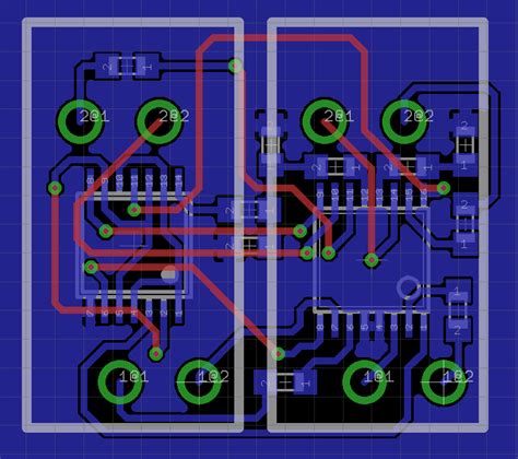
PCB layout refers to the process of arranging electronic components and routing the connections between them on a printed circuit board. The goal of PCB layout is to create a design that is functional, reliable, and manufacturable while also meeting the specific requirements of the intended application.
A typical PCB layout includes the following elements:
- Components: The electronic components that make up the circuit, such as resistors, capacitors, integrated circuits (ICs), and connectors.
- Traces: The conductive paths that connect the components on the PCB.
- Vias: The holes drilled through the PCB to allow traces to connect between layers.
- Pads: The exposed areas of copper on the PCB where components are soldered.
- Silkscreen: The text and symbols printed on the PCB to identify components and provide assembly instructions.
The Importance of Proper PCB Layout Design
Proper PCB layout design is essential for several reasons:
-
Functionality: A well-designed PCB layout ensures that the circuit functions as intended, with minimal signal integrity issues, crosstalk, and electromagnetic interference (EMI).
-
Reliability: Proper component placement and trace routing can help minimize thermal stress, mechanical stress, and other factors that can impact the long-term reliability of the PCB.
-
Manufacturability: A PCB layout that follows design rules and guidelines is easier to manufacture, with fewer defects and higher yields.
-
Cost: An optimized PCB layout can help reduce manufacturing costs by minimizing the size of the board, the number of layers, and the complexity of the assembly process.
PCB Layout Design Tools and Software
To create a PCB layout, designers use specialized software tools that allow them to place components, route traces, and verify the design against a set of design rules. Some of the most popular PCB layout design tools include:
-
Altium Designer: A powerful and feature-rich PCB design tool used by many professional designers.
-
Cadence Allegro: A high-end PCB design solution used in the aerospace, defense, and automotive industries.
-
KiCad: A free and open-source PCB design tool that is popular among hobbyists and small businesses.
-
EAGLE: A widely used PCB design tool that offers a free version for non-commercial use.
-
OrCAD: A comprehensive PCB design solution that includes schematic capture, simulation, and layout tools.
These tools offer a range of features and capabilities, including:
- Schematic capture: The ability to create and edit schematic diagrams of the circuit.
- Component libraries: Extensive libraries of component footprints and symbols.
- Auto-routing: Automated tools for routing traces between components.
- Design rule checking (DRC): Automated checks to ensure that the layout meets the specified design rules.
- 3D visualization: The ability to view the PCB layout in 3D to check for clearances and mechanical fit.

PCB Layout Design Guidelines and Best Practices
To create a successful PCB layout, designers must follow a set of guidelines and best practices that help ensure the functionality, reliability, and manufacturability of the board. Some of the key guidelines include:
Component Placement
- Place components in a logical and organized manner, grouping related components together.
- Consider the flow of signals through the circuit and place components to minimize the length of traces.
- Ensure that components are oriented correctly and have sufficient clearance for assembly and soldering.
Trace Routing
- Use the shortest and most direct path possible for each trace to minimize signal integrity issues and reduce EMI.
- Avoid sharp corners and angles in traces, which can cause signal reflections and EMI.
- Maintain consistent trace widths and spacing to ensure proper impedance and minimize crosstalk.
- Use ground planes and power planes to provide low-impedance return paths for signals and reduce EMI.
Grounding and Power Distribution
- Use a solid ground plane to provide a low-impedance return path for signals and minimize EMI.
- Provide adequate power distribution to all components, using wide traces or power planes to minimize voltage drop and ensure reliable operation.
- Use decoupling capacitors near power pins of ICs to reduce noise and ensure stable power delivery.
Signal Integrity
- Minimize the length of high-speed traces to reduce signal integrity issues such as reflections, ringing, and crosstalk.
- Use appropriate termination techniques, such as series termination or parallel termination, to match the impedance of the trace to the source and load.
- Use differential pairs for high-speed signals to minimize EMI and improve signal quality.
Thermal Management
- Consider the power dissipation of components and provide adequate cooling, such as thermal vias or heatsinks, to prevent overheating.
- Place temperature-sensitive components away from heat-generating components to minimize thermal stress.
Manufacturing Considerations
- Follow the design rules and guidelines provided by the PCB manufacturer to ensure manufacturability and minimize defects.
- Provide adequate clearances and tolerances for component placement, trace routing, and drill holes.
- Use standard component packages and footprints whenever possible to minimize custom tooling and reduce manufacturing costs.

The Benefits of Using a Professional PCB Layout Design Service
While it is possible for individuals and small businesses to design their own PCB layouts using the tools and guidelines mentioned above, there are several benefits to using a professional PCB layout design service:
-
Expertise: Professional PCB layout designers have the knowledge, skills, and experience to create optimized layouts that meet the specific requirements of each project.
-
Time savings: Outsourcing PCB layout design allows businesses to focus on their core competencies while leaving the complex and time-consuming task of PCB layout to the experts.
-
Cost savings: A professional PCB layout design service can help minimize manufacturing costs by creating layouts that are optimized for the specific manufacturing process and volume.
-
Quality assurance: Professional PCB layout designers use industry-standard tools and follow strict quality control processes to ensure that each layout meets the highest standards of functionality, reliability, and manufacturability.
-
Scalability: A professional PCB layout design service can handle projects of any size and complexity, from simple single-layer boards to complex multi-layer designs with high-speed signals and advanced packaging requirements.

Choosing the Right PCB Layout Design Service
When choosing a PCB layout design service, there are several factors to consider:
-
Experience: Look for a service provider with extensive experience in PCB layout design, particularly in the specific industry or application area of your project.
-
Capabilities: Ensure that the service provider has the tools, expertise, and resources to handle your specific project requirements, such as high-speed design, advanced packaging, or flex PCBs.
-
Communication: Choose a service provider that communicates clearly and promptly, and is responsive to your needs and feedback throughout the project.
-
Quality: Look for a service provider with a proven track record of delivering high-quality PCB layouts that meet or exceed customer expectations.
-
Cost: Consider the cost of the service in relation to the value it provides, taking into account factors such as expertise, quality, and turnaround time.
Conclusion
PCB layout design is a critical step in the development of electronic devices, with significant impacts on functionality, reliability, manufacturability, and cost. By following best practices and guidelines, and using the right tools and expertise, it is possible to create optimized PCB layouts that meet the specific requirements of each project.
For businesses and individuals who lack the time, resources, or expertise to design their own PCB layouts, using a professional PCB layout design service can provide significant benefits, including improved quality, faster turnaround times, and lower manufacturing costs.
By choosing the right PCB layout design service and working closely with the service provider throughout the project, businesses can ensure that their electronic products are designed and manufactured to the highest standards of quality and reliability.
FAQ
What is the difference between PCB layout and PCB design?
PCB layout refers specifically to the process of arranging components and routing traces on a PCB, while PCB design encompasses the entire process of designing a PCB, including schematic capture, component selection, and layout.
What are the most important factors to consider when designing a PCB layout?
The most important factors to consider when designing a PCB layout include:
- Component placement and orientation
- Trace routing and spacing
- Grounding and power distribution
- Signal integrity and EMI reduction
- Thermal management
- Manufacturing considerations, such as design rules and tolerances
Can I design my own PCB layout without using a professional service?
Yes, it is possible to design your own PCB layout using specialized software tools and following best practices and guidelines. However, for complex or high-performance designs, or for businesses that lack the time or expertise to design their own layouts, using a professional PCB layout design service can provide significant benefits.
How long does it typically take to complete a PCB layout design?
The time required to complete a PCB layout design varies depending on the complexity of the design, the number of components and layers, and the specific requirements of the project. Simple designs may be completed in a few days, while complex designs may take several weeks or even months.
How much does a professional PCB layout design service typically cost?
The cost of a professional PCB layout design service varies depending on the complexity of the design, the experience and expertise of the service provider, and other factors such as turnaround time and manufacturing requirements. In general, prices can range from a few hundred dollars for simple designs to several thousand dollars or more for complex, high-performance designs. It is important to consider the cost of the service in relation to the value it provides, taking into account factors such as quality, reliability, and manufacturability.
| Factor | Consideration |
|---|---|
| Component Placement | Place components in a logical and organized manner, grouping related components together. |
| Trace Routing | Use the shortest and most direct path possible for each trace to minimize signal integrity issues and reduce EMI. |
| Grounding and Power Distribution | Use a solid ground plane to provide a low-impedance return path for signals and minimize EMI. |
| Signal Integrity | Minimize the length of high-speed traces to reduce signal integrity issues such as reflections, ringing, and crosstalk. |
| Thermal Management | Consider the power dissipation of components and provide adequate cooling, such as thermal vias or heatsinks, to prevent overheating. |
| Manufacturing Considerations | Follow the design rules and guidelines provided by the PCB manufacturer to ensure manufacturability and minimize defects. |