Judy@4pcba.com
7:30 AM - 7:30 PM
Monday to Saturday

Archive: June 30, 2023

What kind of terminal blocks are generally used for PCBs

What kind of terminal blocks are generally used for PCBs

PCB will generally use which kind of terminal blocks which depends on whether it is according to the material to divide or style to divide, if according to the material, should be more copper terminal blocks; according to the style to divide, PCB terminals are divided into plug-in terminal blocks, direct welding terminal blocks, spring-type terminal blocks, fence type terminal blocks, should be plug-in terminal blocks and spring-type terminal blocks more.

  Spring-type terminal block is the use of spring device of the new terminal block, has been widely used in the world of electrical and electronic engineering industry: lighting, elevator lift control, instrumentation, power, chemical and automotive power. Spring type series terminal block metal parts are spring device design, plastic body are used PA66 insulation material. Spring-type series terminal blocks are easy to operate, free maintenance and with gas-tight contact device system, that is durable and reliable and cost-effective.

  Plug-in series terminal blocks PTB by two parts plug-in connection, part of the line will be pressed, and then inserted into the other part, which is soldered to the PCB board. This connection bottom mechanical principle, this anti-vibration design to ensure the long-term airtight connection of the product and the reliability of the use of the finished product. The assembly lugs can be added to both ends of the socket, which largely protect the tabs and prevent poor alignment of the tabs, while the socket design ensures that the socket can be inserted correctly into the female body. The sockets can also have assembly and locking fasteners. The assembly fasteners provide a more secure attachment to the PCB board, while the locking fasteners lock the female and the socket after installation. A variety of socket designs are available with different insertion methods for the masters, such as horizontal, vertical or angled towards the PCB, depending on the customer’s requirements. Both metric and standard wire gauges can be selected.

PCB open and short circuit causes and improvement methods

PCB open and short circuit causes and improvement methods

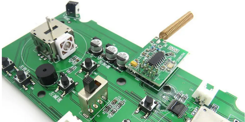
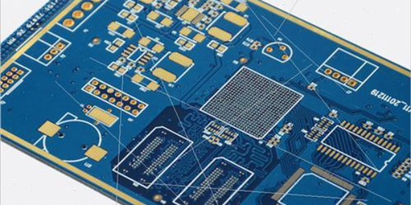
PCB line open, short circuit is the PCB manufacturers almost every day encounter the problem, has been plagued by production, quality management personnel, it caused by the number of insufficient shipments and replenishment, delivery delays, customer complaints, is more difficult to solve the problem of the industry. Ltd. has many years of practice in production, quality, technology and cost control, for PCB open, short circuit problems have accumulated some experience in improving the text is formed to summarize, I hope that we can discuss for your reference.

  First of all, we will cause the main reasons for the PCB open circuit summary categorized as follows:

  Causes of the above phenomenon analysis and improvement methods are categorized as follows:

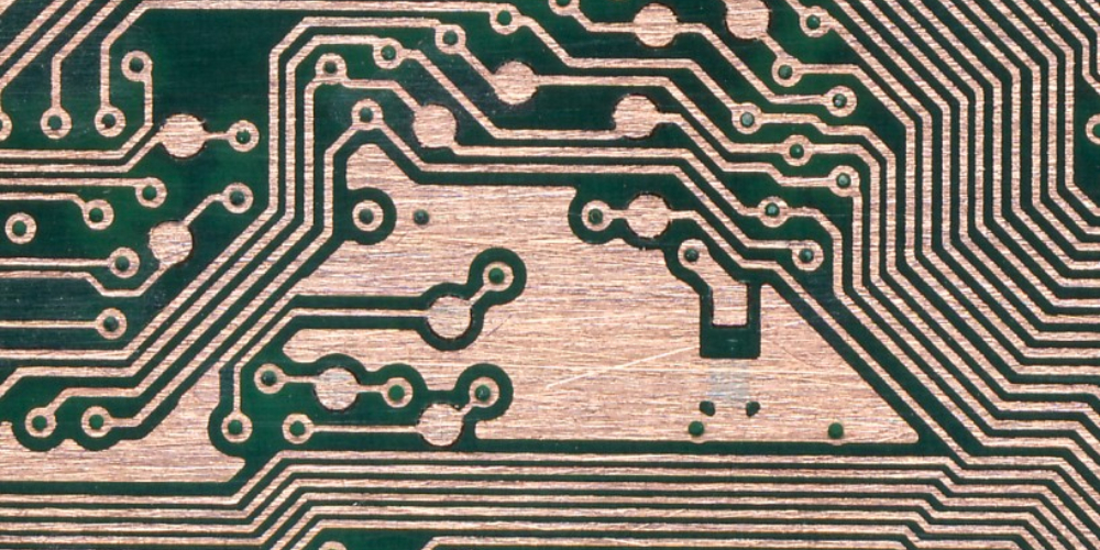
A. Open circuit caused by the exposed substrate:

  1、Copper clad board is scratched before it goes into storage;

  2, copper clad board in the process of opening material was scratched;

  3, copper clad board in the drilling process was scratched by the drill nozzle;

  4, copper clad board in the transfer process was scratched;

  5、The surface copper foil is touched due to improper operation when stacking the board after sinking copper;

  6、The surface copper foil of the production board is scratched when it passes through the horizontal machine.

Improvement methods:

  1, copper clad board in the warehouse before the IQC must carry out random inspection, check whether the board surface is scratched to reveal the base material phenomenon, if there should be timely contact with the supplier, according to the actual situation, to make the appropriate treatment.

  2, copper laminate in the process of opening material is scratched, the main reason is the presence of hard sharps on the table of the open machine, open material when the copper laminate and sharps abrasion caused by copper foil scratches formed by the phenomenon of open base material, so the material must be carefully cleaned before the table, to ensure that the table is smooth and no hard sharps.

  3, copper clad board in drilling by the drill nozzle scratch, the main reason is the spindle clamp nozzle is worn, or clamping nozzle within the debris is not clean, grasping the drill nozzle when the grip is not firm, the drill nozzle did not go up to the top, slightly longer than the length of the set drill nozzle, drilling when lifting the height is not enough, the machine moves when the tip of the drill nozzle scratches copper foil to form the phenomenon of exposed base material.

  a. The chucking nozzle can be replaced by the number of times recorded by grasping the tool or according to the degree of wear of the chucking nozzle;

  b. Clean the chucking nozzle regularly according to the operation procedures to ensure that there is no debris in the chucking nozzle.

  4、The plate is scratched during the transfer process:

  a, handling personnel lifting the board at one time too much, the weight is too large, the board in the handling is not lifted, but dragged up, causing the board corner and the board surface friction and scratched the board surface;

  b, put down the board because not put neatly, in order to rearrange and push the board, causing friction between the board and the board and scratch the board surface.

  5、After sinking copper, full plate plating after stacking the board due to improper operation is scratched:

  After sinking copper, full plate plating storage board, because the board stacked together, there are a certain number of weight is not small, and then put down, the board angle down and coupled with a gravitational acceleration, the formation of a strong impact on the board surface, causing the board surface scratches exposed substrate.

6、The production board is scratched when passing the horizontal machine::

  a, grinding plate machine baffle sometimes touch the surface of the plate, the edge of the baffle is generally uneven and favorable object projection, over the plate when the plate surface is scratched;

  b, stainless steel drive shaft, due to damage into a pointed object, over the plate when the copper surface is scratched and exposed to the base material.

  To sum up, for the phenomenon of scratching in the sunken copper after the base material, if the line is in the form of an open circuit or line gap to show, easy to judge; if the scratching in the sunken copper before the appearance of the base material, but also in the line, after the sunken copper and sunk on a layer of copper, the thickness of the copper foil of the line is significantly reduced, the back open, short circuit test is difficult to detect, so that customers may use because they can not withstand Excessive current and cause the line to be burned off, the potential quality problems and the resulting economic losses are quite large. Second, non-porous open circuit:

  1, sunken copper non-porous;

  2, non-porous caused by oil in the hole;

  3, non-porous caused by excessive micro-etching;

  4, non-porous caused by poor plating

  5、Burning hole or dust plugging hole caused by drilling no hole.

Improvement measures:

  1、Sink copper non-porosity:

  a. Non-porosity caused by the rectifying agent: It is due to the imbalance or failure of the chemical concentration of the rectifying agent. The role of the whole hole agent is to adjust the electrical properties of the insulating substrate on the wall of the hole, in order to facilitate the subsequent adsorption of palladium ions, to ensure complete chemical copper coverage, if the chemical concentration of the whole hole agent is not balanced or failure, will lead to non-porosity.

  b, activator: its main components are pd, organic acids, tin ions and chloride. The pore wall to have the metal palladium uniformly deposited on it is necessary to control all aspects of the parameters, so that it meets the requirements, we now use the activator as an example:

  ①, temperature control at 35 ~ 44 ℃, if the temperature is low caused by the palladium deposited on the density is not enough, chemical copper coverage is not complete; high temperature because the reaction is too fast, the material cost increases.

  ②, the concentration of colorimetric control at 80% to 100%, if the concentration is low, resulting in palladium deposited on the density is not enough, chemical copper coverage is incomplete; high concentration because of the reaction is too fast, the material cost increases.

  ③, in the production process to maintain the activator solution, if the degree of pollution is more serious, it will cause the palladium deposited on the hole wall is not dense, the subsequent chemical copper coverage is not complete.

  c, accelerator: the main component is organic acid, is used to remove the pore wall adsorption of stannous and chloride compounds, revealing the subsequent reaction of the catalytic metal palladium. We now use accelerator, chemical concentration control in 0.35 ~ 0.50N, if the concentration is high to remove the metal palladium, resulting in incomplete coverage of the subsequent chemical copper. If the concentration is low, the removal of pore wall adsorption of tin and chloride compounds is not effective, resulting in incomplete coverage of the subsequent chemical copper.

  d. The control of chemical copper parameters is the key to good or bad chemical copper coverage, taking the parameters of the potion currently used by our company as an example:

①, temperature control at 25 ~ 32 ℃, the temperature is low, the liquid activity is not good, resulting in non-porous; if the temperature exceeds 38 ℃, because the liquid reaction is fast, copper ion release is also fast, easy to cause the plate surface copper particles and rework or even scrap, then the sink copper liquid to be filtered immediately, otherwise the liquid may cause scrap.

  ②, Cu2+ control in 1.5 ~ 3.0g / L, Cu2+ content is low, the liquid activity is not good, will cause poor hole; if the concentration exceeds 3.5g / L, because the liquid reaction is fast, copper ion release is also fast, resulting in plate surface copper particles and rework or even scrap, so the sink copper liquid to immediately filter, otherwise the liquid may cause scrap Cu2+ control is mainly through the addition of sink copper A liquid for control.

  ③, NaOH control at 10.5 ~ 13.0g / L is appropriate, NaOH content is low, the liquid activity is not good, will cause poor porosity NaOH control is mainly through the addition of copper sink B liquid control, B liquid contains the liquid stabilizer, under normal circumstances A liquid and B liquid is 1:1 to add the supplement.

  HCHO control in 4.0 ~ 8.0g / L, HCHO content is low, the liquid activity is not good, resulting in poor porosity, if the concentration exceeds 8.0g / L, because the liquid reaction is fast, the release of copper ions is also fast, resulting in plate copper particles and rework or even scrap, so the copper sink solution to be filtered immediately, otherwise the liquid may cause scrap. HCHO control is mainly through the addition of copper sink C liquid for Control, A liquid also contains HCHO composition of the liquid, so add HCHO, first calculate the amount of HCHO concentration increase when supplementing A liquid.

  ⑤, sink copper load control at 0.15 ~ 0.25ft2 / L, the load is low, the liquid activity is not good, resulting in poor porosity; if the load exceeds 0.25ft2 / L, because the liquid reaction is fast, copper ion release is also fast, resulting in plate surface copper particles and rework or even scrap, so sink copper liquid to be filtered immediately, otherwise the liquid may cause scrap. Production of the first cylinder plate must be used to drag the copper plate, the activity of the copper sink solution to activate the reaction of the subsequent copper sink products, to ensure the density of chemical copper in the hole and improve coverage.

  Suggestions: In order to achieve a balance and stability of the above parameters, the sink copper cylinder to add A, B liquid, should be equipped with an automatic filling machine to better control the chemical composition; at the same time, the temperature also uses automatic control devices to make the sink copper line solution temperature in a controlled state.

2, hole residual wet film oil caused by non-porous:

  a, screen printing wet film when printing a plate scraped once the bottom of the screen, to ensure that the bottom of the screen no oil pile phenomenon exists, under normal circumstances there will be no hole residual wet film oil phenomenon;

  b, screen printing wet film when the use of 68 to 77T screen, if the wrong screen, such as ≤ 51T, the hole may leak into the wet film oil, the development of the oil in the hole may not be clean, the plating will not be plated on the metal layer and caused by non-porous. If the mesh is high, it is possible that the ink thickness is not enough, and the anti-coating is broken by the current when plating, causing a lot of metal spots between the circuits or even lead to short circuit.

  3、Roughening excessive caused by non-porosity:

  a, before the line if the use of chemical roughening plate, the temperature of the roughening solution, concentration, roughening time and other parameters to control, otherwise it is possible that the plate plating hole copper thickness is thin, can not withstand the copper dissolving force of the roughening solution and caused by non-porosity.

  b. In order to strengthen the bonding force between the plating layer and the base copper, the plating pre-treatment should be chemically roughened before plating, so the temperature, concentration, roughening time and other parameters of the roughening solution should be well controlled, otherwise it may also cause the problem of non-porosity.

  4、Plating non-porosity: a. The thickness of the plating is large:

  a, plating when the thickness of the diameter is relatively large (≥ 5: 1), there will be bubbles in the hole, this is because the vibration force is not enough to make the air escape from the hole, it is also impossible to achieve ion exchange, so that the hole is not plated with copper / tin, etching the hole when the copper etched off will cause non-porosity.

  b, the thickness of the diameter is relatively large (≥ 5: 1), electroplating pretreatment due to oxidation in the hole is not clean, electroplating will appear to resist the plating phenomenon, no copper / tin plating or plating on the copper / tin is very thin, etching can not resist the effect of corrosion caused by the hole of copper etched off and caused by non-porosity.

  5、Drill nozzle burn hole or dust plugging hole non-porous

  a, drilling nozzle life is not set, or the use of the drill nozzle wear is more serious, such as gap, not sharp, drilling due to friction and too much heat, resulting in hole wall scorching can not cover the chemical copper and cause no hole.

  b. The suction power of the vacuum machine is not big enough, or the engineering optimization is not done well, and the hole is clogged with dust when drilling, which causes non-porosity due to not sinking on copper when chemical copper is used.

PCB copy process how to properly disassemble the integrated circuit

PCB copy process how to properly disassemble the integrated circuit

In the PCB copy process, we often need to disassemble the circuit board, remove the integrated circuit and other components to create a BOM list, and will be disassembled from the bare board to scan and copy the board. The integrated circuit pins are not only more dense, disassembly is often easy to make mistakes and thus damage the board, resulting in the failure of PCB copy. Therefore, in the process of PCB copy, how to correctly disassemble the integrated circuits on the PCB board becomes an important issue.

Shenzhen RayMing Technology’s senior team of professional PCB copy board companies said that PCB copy board is very much focused on technology and experience, especially in the disassembly of integrated circuits, but also the key to the successful implementation of PCB copy board. The following is Shenzhen RayMing summary of more than a decade of PCB copy board experience, now provides you with several easy and effective methods to disassemble the circuit board for your reference.

A. Solder sucker tin disassembly method

The use of solder absorbers to disassemble the integrated block, which is a common professional method, the use of tools for ordinary suction, soldering soldering iron, the power of more than 35W. When disassembling the integrated block, as long as the heated dual-use soldering iron head on the pins of the integrated block to be disassembled, to be melted solder joint tin is sucked into the fine tin ware, all the pins of the solder sucked after the integrated block can be taken off.

Second, medical hollow pin disassembly method

Take a few medical hollow pins of 8 to 12. When the use of the needle is just the right set of internal warp integration block pins appropriate. Disassembly with a soldering iron to dissolve the pin solder, in time to use the pin set pin, then remove the soldering iron and rotate the pin, and so the solder solidification after pulling out the pin. So the pin is completely separated from the printed board. After all the pins are done once, the integrated block can be easily taken off.

Three, multi-strand copper wire suction tin removal method

It is the use of multi-strand copper core plastic wire, remove the plastic skin, use multi-strand copper core wire (can use short wire head). Before using the multi-stranded copper core wire on the rosin alcohol solution, to be hot soldering iron will be multi-stranded copper core wire into the integrated block pins heated, so that the tin solder on the pins will be adsorbed by the copper wire, suck on the part of the solder can be cut off, repeated several times on the pins can be sucked away all the solder. Conditions can also use the braided wire inside the shield. As long as the solder sucked, with tweezers or a small “a” screwdriver gently pry, the integrated block can be removed.

Four, soldering iron brush with disassembly method

The method is simple and easy, as long as there is a soldering iron and a small brush can be. When disassembling the integrated block, the soldering iron is first heated to reach the melting temperature of the solder on the pins, and then take the opportunity to sweep off the melted solder with a brush. In this way, the pins of the integrated block can be separated from the printed board. The method can be divided into pins or can be carried out separately. Finally, use pointed tweezers or small “a” screwdriver to pry down the integrated block.

Five, increase the solder melting demolition method

The method is a hassle-free method, as long as the integrated block to be disassembled on the pins and then increase some solder, so that the solder joints of each column of pins are connected, so as to facilitate heat transfer, easy to disassemble. When disassembly with a soldering iron each heated column of pins with pointed tweezers or small “a” screwdriver pry a pry, two columns of pins rotating heating, until removed. In general, each column of pins heated twice can be removed.

Thus, although the PCB copy process of disassembling the integrated circuit is easy to make mistakes, but as long as the step-by-step, according to the correct method of disassembly, you can ensure the complete disassembly of the integrated circuit, the successful completion of the PCB copy board to lay a solid foundation.

Of course, in the PCB copy process, in addition to the disassembly of integrated circuits, there are many details that need attention. Shenzhen RayMing has a professional PCB copy team, which has accumulated rich experience in the process of copying boards for more than ten years, and is sincere in solving problems and providing more new strength for the steady development of PCB copy boards in China.

How to choose the right board when PCB copy

How to choose the right board when PCB copy

PCB copy how to choose the right board, choose PCB board must be in the middle of meeting the design requirements and mass production and cost to strike a balance. Design requirements include both electrical and mechanical components. Usually in the design of very high-speed PCB board (greater than GHz frequency) when the material issues will be more important. For example, now commonly used FR-4 material, in a few GHz frequency dielectric loss (dielectric loss) will have a significant impact on signal attenuation, may not be suitable. In terms of electrical, we should pay attention to the dielectric constant (dielectricconstant) and dielectric loss in the designed frequency is suitable.

94HB: ordinary cardboard, not fire-resistant (the lowest grade material, die punching, can not do power supply board)
94V0: flame retardant cardboard (die-punched)
22F: single-sided half glass fiber board (die-punched)
CEM-1: single-sided fiberglass board (must be computer-drilled, can not be die-punched)
CEM-3: double-sided half glass fiber board (except double-sided cardboard belongs to the lowest material of double-sided board, simple double-sided board can use this material, cheaper than FR-4)

FR-4: double-sided glass fiber board

High Tg printed circuit board when the temperature rises to a certain threshold, the substrate will change from “glassy” to “rubbery”, the temperature at this time is called the glass transition temperature (Tg) of the board. In other words, Tg is the maximum temperature (℃) of the substrate to maintain rigidity. That is, ordinary PCB substrate materials at high temperatures, constantly produce softening, deformation, melting and other phenomena, but also in the mechanical and electrical properties of the sharp decline, which affects the service life of the product, the general Tg of the board for more than 130 ℃, high Tg is generally greater than 170 ℃, medium Tg about greater than 150 ℃; usually Tg ≥ 170 ℃ PCB printed board, called high Tg Printed board; substrate Tg improved, the heat resistance of the printed board, moisture resistance, chemical resistance, stability resistance and other characteristics will be increased and improved. the higher the TG value, the better the temperature resistance of the board, especially in the lead-free process, high Tg application more; high Tg refers to high heat resistance. With the leapfrog development of the electronics industry, especially the electronic products represented by the computer, to the development of high functionality, high multi-layer, the need for PCB substrate materials of higher heat resistance as a prerequisite. The emergence and development of high-density mounting technology represented by SMT and CMT make PCB in small aperture, fine line, thinning, more and more inseparable from the support of high heat resistance of the substrate.
So the general FR-4 and high Tg difference: the same at high temperatures, especially under the heat after moisture absorption, its material mechanical strength, dimensional stability, adhesion, water absorption, thermal decomposition, thermal expansion and other differences in various cases, high Tg products are obviously better than ordinary PCB substrate materials.
PCB sheet knowledge and standards currently used in large quantities in our country have the following types of copper-laminate, its characteristics are as follows: copper-laminate types, copper-laminate knowledge, there are various methods of classification of copper-clad foil board. Generally according to the different reinforcing materials of the board, can be divided into: paper-based, glass fiber cloth-based, composite base (CEM series), laminated multilayer board-based and special material-based (ceramic, metal core base, etc.) five categories. If classified according to the different resin adhesives used in the board, the common paper-based CCI. are: phenolic resin (XPc, XxxPC, FR-1, FR a 2, etc.), epoxy resin (FE a 3), polyester resin and other various types.

Common glass fiber cloth-based CCLs include epoxy resins (FR I 4, FR-5), which are the most widely used type of glass fiber cloth base today. There are also other speciality resins (with glass fiber cloth, polybase amide fiber, nonwoven fabric, etc. as added materials): bismaleimide modified triazine resin (BT), polyimide resin (PI), diphenyl ether resin (PPO), maleic anhydride imide – styrene resin (MS), polycyanate resin, polyolefin resins, etc. According to the classification of CCL flame retardant performance, it can be divided into two types of boards: flame retardant (UL94 a VO, UL94 a V1 level) and non-flame retardant (UL94 a HB level). In recent years, as more attention is paid to environmental issues, a new type of CCL without brominated substances has been introduced in the flame retardant CCL, which can be called “green flame retardant CCL”.

With the rapid development of electronic products technology, there are higher performance requirements for cCL. Therefore, the performance classification of CCL is divided into general performance CCL, low dielectric constant CCL, high heat resistance CCL (generally the L of the board is above 150℃), low thermal expansion coefficient CCL (generally used in packaging substrate) and other types. With the development and continuous progress of electronic technology, new requirements for printed board substrate materials are constantly put forward, thus, promoting the continuous development of copper-clad board standards.

How to copy the PCB of the circuit board

How to copy the PCB of the circuit board

  1. Take a PCB board, first of all, you need to record on paper the type of all the components, parameters and location, especially the direction of the diode, tertiary tube, the direction of the IC gap. It is best to use a digital camera to take two photos of the location of the components. Now the more advanced PCB circuit boards are made above the diode, transistor some do not pay attention to simply can not see.
  2. Remove all components, to remove the tin in the PAD hole. Use alcohol to scrub the board clean, and then into the scanner, in the scanner scan to slightly adjust the scan pixels, to get a clearer image of the board. Then lightly sand the top and bottom layers with water gauze paper, sand until the copper film is shiny, put it into the scanner, start PHOTOSHOP, and sweep the two layers in color separately. Note that the PCB must be placed horizontally and vertically in the scanner, otherwise the scanned image will not work.
  3. Adjust the contrast of the canvas, light and darkness, so that the part with copper film and the part without copper film to form a strong contrast, and then turn the figure to black and white, check whether the lines are clear, if not, we must continue to adjust. If clear, save the figure as black and white BMP format two files, if found that the graphics have problems, but also need to use PHOTOSHOP to correct.
  4. the two BMP format files are converted to PROTEL format files, in PROTEL call into the two layers, if the two layers of PAD and VIA position basically overlap, indicating that the first few steps to do a good job, if there are deviations, repeat the third step. Until the match.

PCB, pay attention to the SILK layer, that is, the yellow layer, and then you trace the lines in the TOP layer is, and according to the second step of the drawing to place the device. After drawing the SILK layer will be deleted. Keep repeating until you have drawn all the layers.

PCB and BOT.PCB into PROTEL, combined into one figure is OK. Use a laser printer to print the TOP LAYER, BOTTOM LAYER on a transparent film (1:1 ratio), put the film on that PCB, compare if there is a mistake, if not, even if successful.

PCB copy board and the difference between PCB making

PCB copy board and the difference between PCB making

PCB is a board made according to your own design

Copy board is someone else’s finished board scan, and then copy the software to simulate the wiring, size, etc. made of PCB files, and then according to the PCB file to make the board, copy the board as the name implies is to copy someone else’s design to make the board.

PCB manufacturing is the manufacture of products,

the design of the graphic information (gerber file) into the actual product (PCB board).

Board making is to take the design file to make PCB

PCB copy is to do a good job of people’s PCB board, to copy the GerBer file, PCB manufacturers to use this file to produce PCB boards.

Copy board is the ready-made PCB cut, with a chemical potion treatment to get the design file. That is, know how to connect the lines inside.

Notes for professional circuit board copy

Notes for professional circuit board copy

Professional circuit board copy notes. Now there are more circuit board copy companies, but some of the low prices are generally used to copy the components used in the board and not to build a library to place but with the elements placed, so that the elements placed on the copied board can not be modified and create a network table for secondary development and design, and secondly, there are now many individuals in the copy board, in the absence of quality assurance price than professional circuit board copy company prices will naturally be low, but the board so copied out The quality is not guaranteed.

Generally in the circuit board copy board where there may be problems is to copy the board board and check, we have their own set of perfect procedures to ensure the clarity of the picture. A series of inspection methods after making the file are done by professionals, which greatly ensures the accuracy of the file, and we can provide customers with clear picture files of each layer after the file is made, which can make the circuit board copy board company or individual can also confirm the inspection by themselves.

Before the board is copied, professional personnel must be required to assess the board to be copied, mainly depending on what the board is used for, the function of the board needs to be confirmed before copying whether there is no IC procurement, whether there are ICs need to be decrypted, whether the IC can be decrypted, the general DSP, CPLD and other large scale ICs decryption is relatively difficult, or the price is relatively high, you also need to confirm whether the copy is a high-precision instrument class or the product needs to be adjusted individually. The product needs to be adjusted one by one.

The schematic diagram is drawn based on the network of the circuit board file, not with a multimeter, after drawing and the original network of the circuit board file for comparison, so the connection can be guaranteed to be 100% consistent, some information is not easy to find IC three-level tube circuit board copy company does not give his correct pin definition, but in the circuit board with 1. 2. Therefore, the corresponding pin connections in the circuit board are absolutely correct.

The pcb copy board process to reverse push the schematic

The pcb copy board process to reverse push the schematic

In the study of PCB reverse technology, the reverse schematic is a PCB circuit diagram based on the PCB file diagram reverse or directly depicted from the product object, which aims to illustrate the circuit board principle and operation. And, this circuit diagram is also used to analyze the functional characteristics of the product itself. In the forward design, the development of the product is generally done with the schematic design and then the PCB design based on the schematic.

Whether it is used to analyze the circuit board principles and product operating characteristics in reverse research, or reused as the basis and foundation for PCB design in forward design, PCB schematics have a special role. So, according to the file diagram or physical, how to reverse the PCB schematic, the reverse process has to pay attention to those details?

First, a reasonable division of functional areas

In the reverse design of a PCB board intact schematic, a reasonable division of functional areas can help engineers reduce some unnecessary trouble and improve the efficiency of drawing. Generally speaking, a PCB board with the same function of the components will be arranged centrally, to functionally divide the area can have a convenient and accurate basis for the reverse schematic diagram.

However, the division of this functional area is not arbitrary. It requires engineers to have a certain understanding of electronic circuit-related knowledge. First, find out the core components in a functional unit, and then according to the alignment connection can be followed to find out the other components of the same functional unit, forming a functional partition. The formation of functional partitions is the basis for schematic drawing. In addition, in this process, do not forget to cleverly use the component serial number on the board, they can help you faster functional partitioning.

Second, find the right reference parts

This benchmark can also be said to be the main component PCB network city at the beginning of the schematic drawing with the help of the benchmark, after determining the benchmark, according to the pins of these benchmark to draw, to a greater extent to ensure the accuracy of the schematic.

For engineers, the determination of the benchmark is not a very complicated matter, in general, you can choose to play a major role in the circuit components as the benchmark, they are generally larger, more pins, convenient for drawing, such as integrated circuits, transformers, transistors, etc., can be used as a suitable benchmark.

Third, the correct distinction between lines, reasonable drawing wiring

For the ground, power, signal line distinction, the same need for engineers to have the relevant power knowledge, circuit connection knowledge, PCB wiring knowledge and so on. The distinction of these lines can be analyzed in terms of component connection, line copper foil width, and the characteristics of the electronic product itself.

In wiring drawing, in order to avoid line crossings and interpolations, ground symbols can be used extensively for ground lines, and various lines can be used in different colors to ensure that they are clearly identifiable, and special signs can also be used for various components, and even unit circuits can be drawn separately and then combined at the end.

Fourth, master the basic framework, drawing on similar schematics

For some basic electronic circuit framework composition and schematic drawing, engineers need to master, not only to be able to some simple, classic unit circuit of the basic composition of the form of direct drawing, but also to form the overall framework of the electronic circuit. On the other hand, do not ignore that the same type of electronic products in the schematic diagram has a certain similarity PCB network city, engineers can accumulate experience based on the full reference to similar circuit diagrams to carry out the backpropagation of new product schematic diagrams.

Five, check and optimize

After the completion of the schematic drawing, but also after testing and verification links to say that the reverse design of the PCB schematic end. The nominal values of components sensitive to PCB distribution parameters need to be checked and optimized, according to the PCB file diagram, the schematic diagram for comparative analysis and verification to ensure that the schematic diagram and the file diagram are identical.

If the schematic layout is found to be inconsistent with the requirements in the check, schematic adjustments will be made until it is completely reasonable and standardized, accurate and clear.

28-layer high-density PCB copy board

28-layer high-density PCB copy board

In the domestic companies that have mastered the technology of board copying, especially RayMing Technology’s board copying technology is the most advanced, now on the market many circuit board copying is very “cottage”, only to do the shape of God is not similar, the function of the gap is very large. Shenzhen RayMing Technology has been focusing on PCB design research in recent years, and can carry out secondary development of the original PCB circuit wiring design deficiencies, and can change the design of some special features requested by the customer, mastered the chip decryption software attack, electronic detection attack, fault generation technology and probe technology and many other key technologies, and in the process of program disassembly in accordance with customer wishes In the process of program disassembly, we add the unique product functions accumulated by our company in long-term independent development, and our service is the leader in the industry with accuracy, speed, low error and unique upgrade performance.
  RayMing Technology is experienced in the market
  The field of copy board is also an industry that requires continuous accumulation of experience, if you are involved in an industry for the first time, it is inevitable that the technology is also constrained because of the limitations of the eyes. We are familiar with the needs of consumers in these fields and can make important product upgrades and work with customers to find the right market position for their products.
In addition, RayMing Technology’s services are also one-stop, providing users with the entire process from circuit board copy, production, placement, insertion, soldering, assembly, testing, repair, inspection, packaging to shipping services!

Copy board, also called cloning or imitation, is the reverse technology research of the designed PCB board; the current new definition: in a narrow sense, copy board only refers to the extraction of electronic product circuit board PCB file restoration and the process of using the file for circuit board cloning; in a broad sense, copy board includes not only the technical process of circuit board file extraction, circuit board cloning, circuit board imitation, and so on, but also includes the circuit board In a broader sense, it includes not only the technical process of circuit board file extraction, circuit board cloning, circuit board imitation, but also the modification of circuit board files (i.e. board modification), the extraction of three-dimensional data and model imitation of electronic product form molds (i.e. copy number), the imitation of various electronic components on the circuit board of electronic products, the decryption of encrypted chips or microcontrollers on the circuit board, the disassembly of system software of electronic products, and all the technical processes of electronic product cloning.
Microcontrollers (MCUs) generally have internal EEPROM / FLASH for users to store programs and work data. In order to prevent unauthorized access or copying of the MCU’s internal program, most MCUs come with an encryption lock locator or encrypted bytes to protect the internal program. If the encryption lock positioning is enabled (locked) during programming, the program inside the microcontroller cannot be read directly with a normal programmer, which is called microcontroller encryption or chip encryption. Microcontroller attackers with the help of special equipment or homemade equipment, the use of microcontroller chip design loopholes or software defects, through a variety of technical means, you can extract key information from the chip, access to the program within the microcontroller which is called chip decryption.

RayMing Technology, as an excellent enterprise in the domestic PCB industry, specializes in providing services such as IT software technology development and chip decryption technology, is a professional chip decryption service company, focusing on PCB design and PCB copy board, can provide a full set of good quality and price decryption services and perfect technical support to help enterprises improve their market competitiveness and join the IT development faster and more steadily. fast track.
RayMing Technology Company has first-class technical, production and service talents as well as international advanced production equipment to provide customers with professional, highly efficient and competitively priced various software technologies and PCB design, copy board, production and a series of comprehensive technology development and functional perfection. The software technology provided includes software development and Chineseization technology, software registration decryption and chip decryption technology, microcontroller software and DSP decryption technology, DOS software decryption and Chineseization technology, and can make reliable chip design, wafer foundry, chip imitation and foundry, CPLD decryption, PCB copy board and PCB board drawing design and OEM processing, return schematic and schematic design, and BOM sheet production according to customer requirements. We also provide BOM table production. The company can also provide customers with material procurement services, ODM, OEM and SMT services, as well as functional prototype production services, for enterprise customers to design the original prototype, the original prototype software program and hardware function of the secondary development of a full set of solutions.
RayMing Technology Company adopts IBM management methods to ensure high efficiency and quality services, pays high attention to the company’s technical development, and strives to provide customers with better quality designs, products and services at better prices. In terms of PCB copy, RayMing Technology can provide customers with 1 to 28 layers of high-density PCB copy, even if the customer company only provides a motherboard, it can achieve a one-time copy success, and the high accuracy of the PCB diagram can be confused with the original PCB, and the cost required for this excellent copy is very competitive in the market, helping customers to maximize savings in design costs and research and development time. In terms of IC decryption, with its advanced equipment, technology and talents, RayMing Technology can realize the additions and deletions of the original machine functions according to the customer’s requirements, and provide perfect, high-quality and satisfactory services for customers.
RayMing Technology Company has been specialized in PCB design, PCB copy board and PCB processing electronic products complete solutions for many years, and has been developing and growing, has a skilled and comprehensive variety of functional departments, including PCB technology department, IC decryption department, PCB production department, SMT production department, marketing department and technical support department, from development to promotion to sales, providing one-stop, RayMing Technology has a wide range of business areas, covering almost all electronic products in the field of electronics industry, electronic consumer, electronic commercial, electronic military, etc., and many successful cases for RayMing Technology in the PCB industry has achieved a good reputation. We welcome all customer companies to consult and cooperate with us, and experience the accurate, fast, inexpensive and high-quality services RayMing Technology is dedicated to providing for you!

Corn thresher PCB copy board reverse research

Corn thresher PCB copy board reverse research

Shenzhen RayMing Technology specializes in providing multi-layer PCB copy board, PCB design, chip decryption, prototype production services, etc. Friends who are seeking technical support can be assured to contact us, superb technology, professional team, quality service, to ensure that you enjoy the “technology” value for money service. Based on the principle of “technology for the people”, RayMing Technology will focus on the products that can bring convenience to people’s life and work, and the reverse study of corn thresher PCB copy board is one of the many cases:
I. Working principle
The corn threshing machine, when working, corn is fed from the inlet, corn is impacted in the high-speed rotor and drum, the seeds are separated out by the sieve, the corn cob is discharged from the rear of the machine, corn silk, skin is discharged from the air outlet.
The feed inlet is located in the upper part of the machine cover, the corn cob enters the threshing chamber through the feed inlet, and the corn kernels fall off in the threshing chamber by the impact of the rotor rotating at high speed, and are separated out through the sieve holes, and there is a baffle plate in the lower part of the front of the feed inlet to prevent the corn kernels from splashing and injuring people.


This kind of machine, threshing efficiency is determined by the length and diameter of the drum, users can choose this series of corn threshing machine according to their own threshing efficiency, reasonable. The nail teeth on the rotor are wearing parts, should be checked frequently for wear and tear, when the nail teeth wear a quarter, can be repaired by welding or replaced with new nail teeth, such as repair and replacement of new nail teeth, all must be repaired or replaced to ensure the balance of the rotor; screen is a wearing part, such as screen broken, please replace the new screen.

Second, technical parameters
  Weight of single machine: 27 (kg)
  Main shaft speed: 1300 rpm
  Fan speed: 2200 rpm
Equipped with power: single-phase secondary 2.2 (kw)
Equipped with v-belt: main machine: A1000
Fan:A950
  Production efficiency: 1000kg/h
  Depuration rate: ≥98%
Crushing rate: ≤2%
Three, structural characteristics
Corn threshing machine, the main working parts are installed on the machine rotor, through the rotor high-speed rotation and drum impact and threshing, is a more widely used economic threshing equipment, with small size, light weight, installation, operation, maintenance is simple, high production efficiency and many other advantages.
Corn threshing machine, mainly by the screen on the cover (i.e. drum), rotor assembly, feeding device, frame and other five parts, the screen and cover rotor assembly together to form a threshing chamber, rotor assembly is the main working parts, the threshing of corn in the threshing chamber completed.