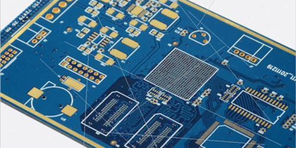
- Take a PCB board, first of all, you need to record on paper the type of all the components, parameters and location, especially the direction of the diode, tertiary tube, the direction of the IC gap. It is best to use a digital camera to take two photos of the location of the components. Now the more advanced PCB circuit boards are made above the diode, transistor some do not pay attention to simply can not see.
- Remove all components, to remove the tin in the PAD hole. Use alcohol to scrub the board clean, and then into the scanner, in the scanner scan to slightly adjust the scan pixels, to get a clearer image of the board. Then lightly sand the top and bottom layers with water gauze paper, sand until the copper film is shiny, put it into the scanner, start PHOTOSHOP, and sweep the two layers in color separately. Note that the PCB must be placed horizontally and vertically in the scanner, otherwise the scanned image will not work.
- Adjust the contrast of the canvas, light and darkness, so that the part with copper film and the part without copper film to form a strong contrast, and then turn the figure to black and white, check whether the lines are clear, if not, we must continue to adjust. If clear, save the figure as black and white BMP format two files, if found that the graphics have problems, but also need to use PHOTOSHOP to correct.
- the two BMP format files are converted to PROTEL format files, in PROTEL call into the two layers, if the two layers of PAD and VIA position basically overlap, indicating that the first few steps to do a good job, if there are deviations, repeat the third step. Until the match.
PCB, pay attention to the SILK layer, that is, the yellow layer, and then you trace the lines in the TOP layer is, and according to the second step of the drawing to place the device. After drawing the SILK layer will be deleted. Keep repeating until you have drawn all the layers.
PCB and BOT.PCB into PROTEL, combined into one figure is OK. Use a laser printer to print the TOP LAYER, BOTTOM LAYER on a transparent film (1:1 ratio), put the film on that PCB, compare if there is a mistake, if not, even if successful.