Judy@4pcba.com
7:30 AM - 7:30 PM
Monday to Saturday

Archive: June 15, 2023

DDS chip

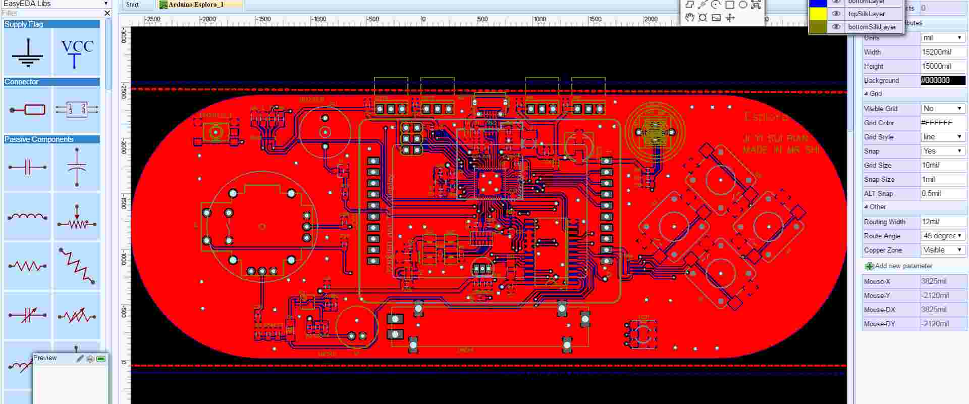
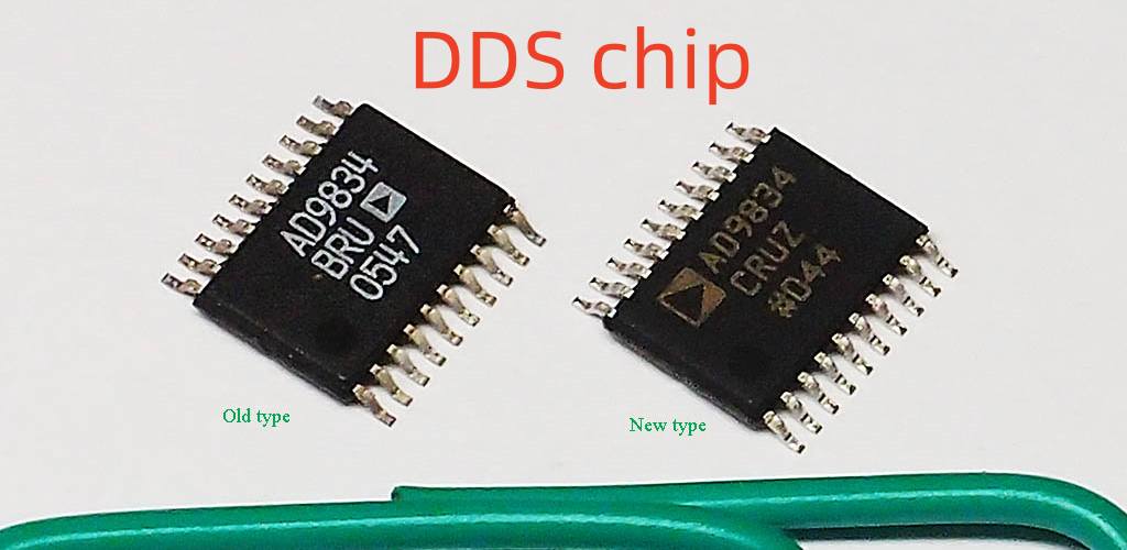
DDS chip decryption and PCB copy technology

DDS chip and PCB copy plays an important role in signal transmission, the company has successfully mastered the DSP Builder sine signal source optimization technology, now the technical principles of the technology described below:

The method of realizing the signal source is frequency synthesis method, in which the direct digital frequency synthesis method is the third generation frequency synthesis technology with the rapid development of electronic technology following the direct frequency synthesis method and the indirect frequency synthesis method. DDS is an all-digital technology that synthesizes the required frequency directly from the phase concept. It has the advantages of short frequency conversion time, high frequency resolution, continuous phase change, low phase noise and low drift, easy integration, adjustment, quadrature Output and other advantages. In recent years, DDS technology in frequency synthesis, communications, radar, electronic warfare, instrument testing and other fields are widely used. Currently dedicated DDS chip signal waveform, function and control mode fixed, often can not meet the specific needs. Field Programmable Gate Array (FPGA) devices are large, fast and programmable hardware features, and the development cycle is short, easy to upgrade, it is very suitable for the realization of DDS.

The basic principle of DDS and PCB copy

The structure of the DDS consists of a phase accumulator, a phase modulator, a waveform memory ROM and a D / A converter, which was proposed by Tierney, Rader and Gold in 1971. A sinusoidal signal generator structure shown in Figure 1. Phase accumulator is the core of the entire DDS, complete the phase accumulation operation, it is the input phase increment B △ θ. Each time the phase accumulator overflows, it represents a complete waveform in the output ROM. The phase modulator receives the phase output of the phase accumulator. Plus a phase offset for the phase modulation of the signal. The sine ROM lookup table completes the phase-to-amplitude conversion, and its input is the output of the phase modulator, which is the address of the ROM.

Fo is the output frequency, the value of fo is determined by fclk and B △ θ: fo = fclk × B △ θ / 2N. According to the Nyquist sampling law, the highest output frequency is half the clock frequency, ie fo = fclk / 2. Practical application, the general take fo ≤ 40% fclk. The frequency resolution of the DDS is measured by the frequency input value step by step, which means Δf = fclk / 2N (by default, the ROM stores the entire period signal waveform). It can be seen that the smaller the △ f, the higher the DDS output accuracy.

2 DDS accuracy improvement program

The ROM lookup table is actually a read-only memory that stores the amplitude of the sinusoidal signal sampling point and converts the input sequence into the amplitude code of the sinusoidal signal. ROM lookup table address bits M the number of bits closer to the phase accumulator N, the smaller the number of bits discarded by phase addressing, the smaller the phase truncation error, but the size of the ROM table will vary with the number of bits Increase the index into the incremental relationship. Therefore, in order to use the smaller ROM to meet the signal performance, the optimization method must be used to compress the ROM.

2.1 sine wave characteristics  and PCB copy

The known sine wave has the following relationship:

It can be seen that the [π, 2π] interval of the waveform can be obtained by [0, π] interval waveform conversion. Furthermore, [π, 2, π], [π, 3π / 2], [3π / 2], [π, 2, π], [π, 2, π] 2π] The three interval waveforms can be obtained by converting the waveforms in the [0, π / 2] interval.

2.2 ROM Builder based on the ROM optimization program

IC Crack Service
IC Crack Service

From the above analysis of the characteristics of the sine wave can be found in the lookup table ROM only stores [O, π] or [0, π / 2] interval of the waveform can be complete cycle of the sinusoidal signal. So that the effective use of the ROM storage interval, improve the storage efficiency. For the case where the [O, π] interval waveform is stored in the ROM, the sine wave can be synthesized into the [0,2π] interval by using the most significant bit of the phase modulator output as a sign bit. In the case where the [0, π / 2] interval waveform is stored in the ROM, the sine wave is synthesized into the [O, π] interval by using the second order judgment quadrant of the phase modulator output; the highest bit is the sign bit, and the sine wave is synthesized To the [0,2π] range. Figure 2 shows the system model for generating sinusoidal signal generators with DSP Builder when storing [O, 2π], [0, π], [O, π / 2] interval waveforms in ROM.

Where WORD is the phase word input and its value is set to O; FWORD is the frequency word input with the value set to 9000000; AWORD is the amplitude control input with the value set to 50; adder is the phase accumulator; adderl is the phase modulator. LUT2, LUT2, LUT3 are ROMs with the same memory space storing [O, 2π], [O, π], [0, π / 2] interval sinusoidal signals, respectively. The module parameters “MATLAB Array” are set to:

In addition, it should be noted that the role of the subsystem controller is to determine the quadrant, the LUT3 sine wave into the [0, π] range.

2.3 Simulation analysis

Figure 3 shows the waveforms of the three outputs OUT1, OUT2, OUT3 in the system model of Figure 2. As can be seen from Figure 3, OUT2 frequency is OUTl 1/2, and OUT3 frequency is OUT2 1/2. This indicates that OUT3 has the highest frequency resolution, 0UT2 times, OUTl lowest. It can be obtained, with the same address input ROM, in the same storage space size, the storage sine wave interval is smaller, the output sinusoidal signal frequency resolution is higher, that is, the higher the output accuracy. Therefore, with the same ROM, when the 1/4 cycle sinusoidal signal is stored, the synthesized sinusoidal signal has a high accuracy.

3 signal source FPGA implementation  and PCB copy

Matlab / Simulink on the design of the DDS system to compile, by calling DSP Builder’s SignalCompiler tool can be directly generated Quartus Ⅱ project files, and then call Quartus Ⅱ complete synthesis, netlist generation and adaptation, until the completion of FPGA configuration download process.

The design of the FPGA chip is used APEX20K series device EP20K200FC484. The resulting digital output can be output to the SRAM chip, and then uploaded to the computer for digital signal analysis, analog output through the HP oscilloscope test. Figure 4 shows the results of the simulation with Quartus II. In the figure, clock is the system clock, sclrp is the high level reset signal, PWORD, FWORD, AWORD are set to decimal numbers 0,9000000 and 50 respectively. The simulation results of the three outputs OUT1, OUT2 and OUT3 and Matlab / Simulink are basically the same in phase, frequency and amplitude. Experiments show that the use of FPGA designed by the DDS to meet the performance conditions, saving the chip resources, improve the accuracy of the output.

Protel-PCB

The skill of Protel 2023 in the PCB Reverse

Advantage of Protel 2023 in PCB Reverse Engineering Service:
Use of high-end wiring technology, complex and innovative layout of the circuit board; Through the rigid-flex board design, to help you have been in the forefront of new technology; Get the best quotes and availability analysis from your most trusted component suppliers; Use centralized component library management, and work with design data that you trust from a single source.

1, in the panel display mode of operation, what skills and need to pay attention to the place?

A variety of display mode of operation, will automatically hide or lock display mode into a floating display is relatively easy, and in turn, the operation is not so simple, need to pay attention to the following aspects.

① When you only want to operate on a panel, drag the mouse should hold the panel on the border panel name, and can not hold the blank area of ​​the border, if holding down the blank area will be the location of all panels operate.

② panel in order to restore the lock or hide the display state, you must check 【Allow Dock】 【Vertically】 or 【Allow Dock】 【Horizontally】 or two selected at the same time, because most of the panel is placed vertically, so the general choice 【Allow Dock 】 【Vertically】. Pcb copy board

③ When you do not want to display more than one panel at the same time in a region, but can be switched in the form of labels, drag the panel should be dragged to the panel label position, when the ▲ logo, release the left mouse Button.

④ Dashed box that appears when the operation is successful.

⑤ in the panel management, the user can open the commonly used panel, do not often use the panel should be closed or hidden, when used to open, this can make the interface clean and tidy.

2, add the library file dialog box [Move Up] and [Move Down] button What is the role?

These 2 buttons are very useful. When you add a lot of library components, select one of them, and then press the [Move Up] or button to move the library up and down. Because the search of the elements in the order of the list in the model link test by the library file, a reasonable arrangement will save a lot of time. The search order for each tag is the [Project] tab, the [Installed] tab, and the [Path] tab.

3, Protel 2023 only supports 90 degree turning of the wire it?

Protel 2023 supports six wire transition modes: 90 ° corner start, 90 ° corner end, 45 ° corner start, 45 ° corner end, any angle, 90 ° corner automatically draws the wire connection between two points. Press 【Space】 key to switch between the two modes of each angle. Press 【Shift】 + 【Space】 to switch between different angle modes. You can observe the wire placement mode in the status bar. On the other hand, the movement of the fixed point can also change the angle of the wire turning.

4, the bus line is divided into several angle mode?

There are four kinds of angle mode, the rotation point as the center, starting with -45 degrees, followed by an increase of 90 degrees, namely -45 degrees, 45 degrees, 135 degrees, 225 degrees. Press the [Space] key to toggle between the four angle modes in the counterclockwise direction, press the [X] key to switch between the two modes with the Y axis as the center, and press the Y key to move the X axis 2 modes. You can observe the placement mode of the bus branch line in the status bar.

5, placing the power symbol need to pay attention to what the problem in actual PCB reverse process?

Need to pay attention to the following three questions.

① in a schematic file, as long as they have the same Net, all of these power will be in the same network, there is electrical connection characteristics.

The symbol style of the power port changes the appearance of the symbol and does not change its electrical connection characteristics.

③ When the schematic diagram of some of the components of the power pin is hidden, the system default to connect to the same Net power port.

6, in the network label placement, what needs to pay attention to the problem?

[Project has a problem is very important. Here we are talking about “have the same network label in the same network” is conditional, that can only guarantee in the schematic in the same network. If a project contains many schematics, such as hierarchical schematic design, to ensure that the different network labels in the schematic can be in the same network, you need to click the [Project] Options …】 menu item, open the [Project Options …] Dialog box, and then select the [Option] tab, in the [Net Identifier Scope] drop-down list box, select [Global] an item.

7, the circuit port placement need to pay attention to what issues?

Need to pay attention to the following four questions.

① In the same schematic, electrical connections are available for circuit ports with the same name.

The port’s Style attribute is independent of the IO Type attribute. For example, a port with the Left and Right property of the Style property does not mean that the IO Type attribute is Bidirectional.

③ When you need to compile or generate a network table, the relationship between the circuit port and the circuit block diagram can be done by clicking the [Project] [Project Options] menu item, select the [Options] tab, in the [Net Identifier Scope] List box.

④ The name of the circuit port is not used to name the network, which means that the system will automatically for the network (which can be in the navigation panel Net view) named.

Protel 2023 software is an excellent tool in PCB design and PCB reverse. 

IC Chip Photography

MC68HC705XX series chip decryption

MC68HC705XX microcontroller with on-chip FLASH, with FLASH memory on-line programming and confidentiality function (FLASH programming / investigation of the voltage generated by the chip internal charge pump), after programming the FLASH bit will be set to 0, after the FLASH bit will be 1, FLASH The encryption feature of the memory prevents unauthorized users from viewing the contents of the FLASH memory.

The following dragon people successfully realize the technological breakthrough MOTOROLA microcontroller model, we can now for the following microcontroller models to provide efficient and reliable decryption services:

    68HC711XX series

68HC711E9MFN2 68HC711E9MFNE2 68HC711E9VFNE2

68HC711E9VFN2 68HC705C4A 68HC705C4

68HC705C8 68HC711E9VFN2 68HC705C8A

68HC705C9 68HC705C9A 68HC705

68HC705J1A 68HC705SR3 …

MC56F8XX series

MC56F8013VFAE MC56F8014VFAE MC56F8023MFAE

MC56F8023VFAE MC56F8025VLD MC56F8036MFAE

MC56F8036VFAE MC56F8037VLH MC56F8122VFA

MC56F8122VFAE MC56F8123VFB MC56F8123VFBE

MC56F8322MFA60 MC56F8322MFAE MC56F8322VFA60

MC56F8322VFAE MC56F8323MFB60 MC56F8323MFBE

MC56F8323VFB60 MC56F8323VFBE …

MC68HC705XX series

MC68HC11P2 (2E74J) MC68HC711P2 (1E53M) MC68HC705C4

MC68HC705C8A MC68HC705C4A MC68HC705C8A

MC68HC705C9 MC68HC705C9A MC68HC705SR3

MC68HC705 MC68HC705J1A MC68HC705B16

MC68HC705X16 MC68HC705B32 MC68HC705X32

MC68HC705B6 MC68HC05B8 MC68HC05B16

MC68HC705X16 MC68HC05B32 MC68HC05X32

MC68HC705H12 (0H57A) MC68HC705B16N MC68HC705B5

MC68HC705J2 MC68HC705KJ1 MC68HC705P6

MC68HC705P9 MC68705R3 MC68705R5

MC68705U3 MC68705U5 XC68HC705P6A (CDW)

MC68HC11XX series

MC68HC11A8 (AB95T) MC68HC11A8 (C96N) MC68HC11E9 (1B60R)

MC68HC11A8 (D26E) MC68HC11E20 (3E22B) MC68HC11E9 (D82R)

MC68HC11E9 (E22B) MC68HC11E9 (E28B) MC68HC11EA9 (2D47J)

MC68HC11F1 (E87J) MC68HC11F1 (2F37E) MC68HC11K1 (2D58N)

MC68HC11K4 (1E62H) MC68HC11K4 (OE75J) MC68HC11KA4 (1E59B)

MC68HC11KS4 (0E57S) MC68HC11KS2 (0H95B) MC68HC11KS4 (0F60M)

MC68HC11A0 MC68HC11A1 MC68HC11E1

MC68HC11P1 …

MC68HC711XX series

MC68HC711E20 (1H19S) MC68HC711E9 (4K81H) MC68HC711E9 (5C47M)

MC68HC711K4 (K59D) MC68HC711EA9 (0D46J) MC68HC711PH8 (0H30R)

MC68S711E9 (5C47M) MC68HC711KS8 (1H96P) MC68HC711D3

MC68HC711E20 MC68HC711E9 MC68HC711E9CFN2

MC68HC711E9CFN (4.5V) MC68HC711E9CFN3 MC68HC711K4

MC68HC711E9CFNE2 MC68HC711E9CFNE3 MC68HC711E9-FN

MC68HC711KA2 MC68HC711KA4 MC68HC711KS2

MC68HC711L6 XC68HC711D3 …

MC68HC81XX series

MC68HC811E2MP2 MC68HC811E2CP2 MC68HC811E2

MC68HC811E2P2 MC68HC811E2VP2 MC68HC812A4CPV

MC68HC812A4CPVE MC68HC812A4MPV …

MC68HC908XX series

MC68HC908AS60 (3J74Y) MC68HC908AZ60 (4J74Y) MC68HC908AZ60 (2J74Y)

MC68HC908AS60A (1L87J) MC68HC908AZ60A (3K85K) MC68HC908AS20 (0H94K)

MC68HC908AZ60 (1J35D) MC68HC908AZ32 (0J66D) MC68HC908AZ32 (1H56A)

MC68H908AZ32A (1L52H) MC68HC908AB32 (3K56G) MC68HC908QT3

MC68HC908QT1 MC68HC908QT2 MC68HC908QT4

MC68HC908QY1 MC68HC908QY2 MC68HC908QY3

MC68HC908QY4 MC68HC908JK1 MC68HC908JK3

MC68HC908AP16CB MC68HC908AB32MFU MC68HC908LK24

MC68HC908AB32CFU MC68HC908AP16CFA MC68HC908JK8

MC68HC908AP16CFB MC68HC908AP32CB MC68HC908LK24

MC68HC908AP32CF MC68HC908AP32CFB MC68HC908AP64CB

MC68HC908AP64CFA MC68HC908AP64CFB MC68HC908AP8CB

MC68HC908AP8CFA MC68HC908AP8CFB MC68HC908AS32A

MC68HC908BD48IB MC68HC908BD48IFB MC68HC908EY16CFA

MC68HC908EY16MFA MC68HC908EY16VFA MC68HC908EY8CFA

MC68HC908EY8MFA MC68HC908EY8VFA MC68HC908GP32

MC68HC908GR16CFA MC68HC908GR16CFJ MC68HC908GR16MFA

MC68HC908GR16MFJ MC68HC908GR16VFA MC68HC908GR4CDW

MC68HC908GR16VFJ MC68HC908GR4CFA MC68HC908GR4CP

MC68HC908GR4MDW MC68HC908GR4MFA MC68HC908GR4MP

MC68HC908GR4VDW MC68HC908GR4VFA MC68HC908GR4VP

MC68HC908GR8CDW MC68HC908GR8CFA MC68HC908GR8CP

MC68HC908GR8MDW MC68HC908GR8MFA MC68HC908GR8MP

MC68HC908GR8VDW MC68HC908GR8VFA MC68HC908GR8VP

MC68HC908GT16 MC68HC908GT8CB MC68HC908GT8CFB

MC68HC908GZ16 MC68HC908GZ32 MC68HC908GZ48 MC68HC908GZ48 MC68HC908GZ48

MC68HC908GZ60 MC68HC908GZ8 MC68HC908JB12

MC68HC908JB16 MC68HC908JK1ECDW MC68HC908JB8

MC68HC908JK1CDW MC68HC908JK1CP MC68HC908JB8

MC68HC908JK1ECP MC68HC908JK1EMDW MC68HC908JK1EMP

MC68HC908JK1MDW MC68HC908JK1MP MC68HC908JK3CDW

MC68HC908JK3CP MC68HC908JK3ECDW ​​MC68HC908JK3ECP

MC68HC908JK3EMDW MC68HC908JK3EMP MC68HC908JK3MDW

MC68HC908JK3MP MC68HC908JK8 MC68HC908JK8

MC68HC908JL3CDW MC68HC908JL3CFA MC68HC908JL3CP

MC68HC908JL3ECDW ​​MC68HC908JL3ECFA MC68HC908JL3ECP

MC68HC908JL3EMDW MC68HC908JL3EMFA MC68HC908JL3EMP

MC68HC908JL3MDW MC68HC908JL3MFA MC68HC908JL3MP

MC68HC908LB8CDWE MC68HC908LB8MDWE MC68HC908LB8CPE

MC68HC908LB8MPE MC68HC908LB8VDWE MC68HC908JL8

MC68HC908LB8VPE MC68HC908LD60IFU MC68HC908KX8

MC68HC908LD64IFU MC68HC908LJ12CFB MC68HC908KX2

MC68HC908LJ12CFBE MC68HC908LJ12CFU MC68HC908LJ12CFU

MC68HC908LJ12CFUE MC68HC908LJ12CPB MC68HC908LJ12CPBE

MC68HC908LJ24CFQ MC68HC908LJ24CFQE MC68HC908LJ24CFU

MC68HC908LJ24CFUE MC68HC908LJ24CPB MC68HC908LJ24CPBE

MC68HC908LJ24CPK MC68HC908LJ24CPKE MC68HC908LK24CFQ

MC68HC908LK24CFQE MC68HC908LK24CFU MC68HC908LK24CFUE

MC68HC908LK24CPB MC68HC908LK24CPBE MC68HC908QB4

MC68HC908LK24CPK MC68HC908LK24CPKE MC68HC908QB8

MC68HC908LV8CPBE MC68HC908MR16 MC68HC908MR32

MC68HC908QC16 MC68HC908QC4 MC68HC908QC8

MC68HC908QT1ACFQE MC68HC908QT1AMFQE MC68HC908QF4

MC68HC908QT1AVFQE MC68HC908QT1CDW MC68HC908QL2

MC68HC908QT1CFQ MC68HC908QT1CP MC68HC908QL3

MC68HC908QT1MDW MC68HC908QT1MFQ MC68HC908QL4

MC68HC908QT1MP MC68HC908QT1VDW MC68HC908QT1VFQ

MC68HC

PCBA reverse

PCBA Clone Industry Is Developing Steadily

Although there are different voices on PCBA clone, there is no doubt that PCBA clone technology is widely applied and has great impact on the development of a country and other industries. PCB clone is widely used in many fields, especially electronics industry, so PCB clone industry attracts much attention from investors and insiders.

Today, China’s electronics and circuit board industries develop very fast; furthermore, the government pays much attention to electronics field, issuing some measures to promote development, which will drive the development of PCBA clone field. Some experts said that PCBA clone trended to grow continuously in the near future. PCB clone’s development also depends on consumers’ demand. As improvement of living standards, people’s living needs are increasing and more and more high-end electronic products are developed, which is also another factor driving the industry’s development. In a word, PCBA clone industry posts a rosy prospect in the overall.

However, China’s PCBA copy technology lags behind some developed countries. Despite manufacturing country, for circuit board production, China has an advantage in numbers, but more efforts must be made to improve quality. Therefore, circuit board copy companies have to enhance technology and change corporate management mode, thus the companies can enhance their competitiveness.

Actually, a lot of companies have changed their business mode. According to market demand, not only do some companies offer PCBA clone service, but also offer PCB design, chip decryption, SMT processing, prototype production and so on, which is called one-stop service. DragonMen is the first company to provide customers with one-stop service in PCB clone industry. It’s believed that PCBA clone industry will be better and better.

PCB copy board concrete steps

PCB copy board concrete steps

The first step is to get a piece of PCB, first in the paper to record all elements of the model, parameters, as well as the location, especially the diode, the direction of the triple tube, the direction of the IC gap.It is better to digital camera two pictures from a location.Now the PCB more do more advanced the diode triode, some do not pay attention to don’t see above.

The second step, tear down all laminated copy board, the tin in the PAD holes and be removed.PCB clean with alcohol, and then put into the scanner, the scanner to scan when need somewhat higher scan pixels, in order to get a clear image.Yarn paper will top and bottom with water slightly grinding, polishing to copper film, into the scanner, start PHOTOSHOP, knocked two layers respectively into in color mode.Note that the PCB must be horizontal even vertical, put in the scanner or scanning image is unusable.

The third step, adjust the contrast of the canvas, the contrast, the copper film part of and not part of the copper film contrast, then the first figure to black and white, check whether the line is clear, if not clear, repeat this step.If clear, will survive for the black and white TOP. The BMP file format of BMP and BOT. BMP, if found problems graphics can also repair and correction in PHOTOSHOP

The fourth step, the two BMP format into PROTEL format file, respectively in PROTEL transfer into two layers, such as a two layer of the PAD and the location of the VIA basic coincidence, that several steps before doing very well, if there is a deviation, then repeat step 3.So PCB copy board is a very need patience work, because a little problem will affect the quality and copy the board after the match.

Fifth, TOP. The TOP layer of BMP can be converted to PCB, be careful to into a SILK layer, the layer is yellow, then you are in the TOP layer is tracing, and drawing device according to the second step.After the draw will delete the SILK layer.Repeated know to draw all the layers.

Step 6, TOP in PROTEL PCB and BOT. PCB paged, into a graph with respect to OK.

Step 7, the TOPLAYER with laser printers, BOTTOMLAYER respectively printed on transparent film (1:1 ratio), put the film on the PCB, compare the errors, if yes, you’re done.

A and the original plate the same copy board was born, but it is only half done.Test, test copy plate electronic technology performance is same as the original plate.If it is completed. Note: if it is a multilayer and careful polishing to the lining of the inside, at the same time, repeat steps, the third to the fifth copy board graphic name is different, of course, want to be decided according to the number of layers, the general double panel is much simpler than a multilayer copy board, multilayer copy plate prone to alignment, so profes sional copy board look and careful (including internal guide hole and guide hole is not easy to appear problem).