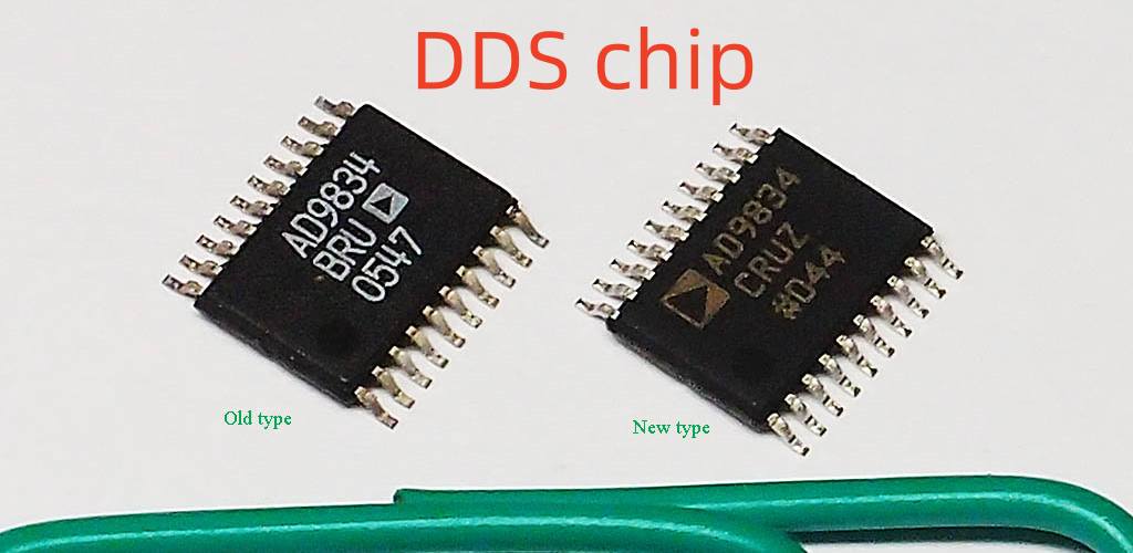
DDS chip and PCB copy plays an important role in signal transmission, the company has successfully mastered the DSP Builder sine signal source optimization technology, now the technical principles of the technology described below:
The method of realizing the signal source is frequency synthesis method, in which the direct digital frequency synthesis method is the third generation frequency synthesis technology with the rapid development of electronic technology following the direct frequency synthesis method and the indirect frequency synthesis method. DDS is an all-digital technology that synthesizes the required frequency directly from the phase concept. It has the advantages of short frequency conversion time, high frequency resolution, continuous phase change, low phase noise and low drift, easy integration, adjustment, quadrature Output and other advantages. In recent years, DDS technology in frequency synthesis, communications, radar, electronic warfare, instrument testing and other fields are widely used. Currently dedicated DDS chip signal waveform, function and control mode fixed, often can not meet the specific needs. Field Programmable Gate Array (FPGA) devices are large, fast and programmable hardware features, and the development cycle is short, easy to upgrade, it is very suitable for the realization of DDS.
The basic principle of DDS and PCB copy
The structure of the DDS consists of a phase accumulator, a phase modulator, a waveform memory ROM and a D / A converter, which was proposed by Tierney, Rader and Gold in 1971. A sinusoidal signal generator structure shown in Figure 1. Phase accumulator is the core of the entire DDS, complete the phase accumulation operation, it is the input phase increment B △ θ. Each time the phase accumulator overflows, it represents a complete waveform in the output ROM. The phase modulator receives the phase output of the phase accumulator. Plus a phase offset for the phase modulation of the signal. The sine ROM lookup table completes the phase-to-amplitude conversion, and its input is the output of the phase modulator, which is the address of the ROM.
Fo is the output frequency, the value of fo is determined by fclk and B △ θ: fo = fclk × B △ θ / 2N. According to the Nyquist sampling law, the highest output frequency is half the clock frequency, ie fo = fclk / 2. Practical application, the general take fo ≤ 40% fclk. The frequency resolution of the DDS is measured by the frequency input value step by step, which means Δf = fclk / 2N (by default, the ROM stores the entire period signal waveform). It can be seen that the smaller the △ f, the higher the DDS output accuracy.
2 DDS accuracy improvement program
The ROM lookup table is actually a read-only memory that stores the amplitude of the sinusoidal signal sampling point and converts the input sequence into the amplitude code of the sinusoidal signal. ROM lookup table address bits M the number of bits closer to the phase accumulator N, the smaller the number of bits discarded by phase addressing, the smaller the phase truncation error, but the size of the ROM table will vary with the number of bits Increase the index into the incremental relationship. Therefore, in order to use the smaller ROM to meet the signal performance, the optimization method must be used to compress the ROM.
2.1 sine wave characteristics and PCB copy
The known sine wave has the following relationship:
It can be seen that the [π, 2π] interval of the waveform can be obtained by [0, π] interval waveform conversion. Furthermore, [π, 2, π], [π, 3π / 2], [3π / 2], [π, 2, π], [π, 2, π] 2π] The three interval waveforms can be obtained by converting the waveforms in the [0, π / 2] interval.
2.2 ROM Builder based on the ROM optimization program

From the above analysis of the characteristics of the sine wave can be found in the lookup table ROM only stores [O, π] or [0, π / 2] interval of the waveform can be complete cycle of the sinusoidal signal. So that the effective use of the ROM storage interval, improve the storage efficiency. For the case where the [O, π] interval waveform is stored in the ROM, the sine wave can be synthesized into the [0,2π] interval by using the most significant bit of the phase modulator output as a sign bit. In the case where the [0, π / 2] interval waveform is stored in the ROM, the sine wave is synthesized into the [O, π] interval by using the second order judgment quadrant of the phase modulator output; the highest bit is the sign bit, and the sine wave is synthesized To the [0,2π] range. Figure 2 shows the system model for generating sinusoidal signal generators with DSP Builder when storing [O, 2π], [0, π], [O, π / 2] interval waveforms in ROM.
Where WORD is the phase word input and its value is set to O; FWORD is the frequency word input with the value set to 9000000; AWORD is the amplitude control input with the value set to 50; adder is the phase accumulator; adderl is the phase modulator. LUT2, LUT2, LUT3 are ROMs with the same memory space storing [O, 2π], [O, π], [0, π / 2] interval sinusoidal signals, respectively. The module parameters “MATLAB Array” are set to:
In addition, it should be noted that the role of the subsystem controller is to determine the quadrant, the LUT3 sine wave into the [0, π] range.
2.3 Simulation analysis
Figure 3 shows the waveforms of the three outputs OUT1, OUT2, OUT3 in the system model of Figure 2. As can be seen from Figure 3, OUT2 frequency is OUTl 1/2, and OUT3 frequency is OUT2 1/2. This indicates that OUT3 has the highest frequency resolution, 0UT2 times, OUTl lowest. It can be obtained, with the same address input ROM, in the same storage space size, the storage sine wave interval is smaller, the output sinusoidal signal frequency resolution is higher, that is, the higher the output accuracy. Therefore, with the same ROM, when the 1/4 cycle sinusoidal signal is stored, the synthesized sinusoidal signal has a high accuracy.
3 signal source FPGA implementation and PCB copy
Matlab / Simulink on the design of the DDS system to compile, by calling DSP Builder’s SignalCompiler tool can be directly generated Quartus Ⅱ project files, and then call Quartus Ⅱ complete synthesis, netlist generation and adaptation, until the completion of FPGA configuration download process.
The design of the FPGA chip is used APEX20K series device EP20K200FC484. The resulting digital output can be output to the SRAM chip, and then uploaded to the computer for digital signal analysis, analog output through the HP oscilloscope test. Figure 4 shows the results of the simulation with Quartus II. In the figure, clock is the system clock, sclrp is the high level reset signal, PWORD, FWORD, AWORD are set to decimal numbers 0,9000000 and 50 respectively. The simulation results of the three outputs OUT1, OUT2 and OUT3 and Matlab / Simulink are basically the same in phase, frequency and amplitude. Experiments show that the use of FPGA designed by the DDS to meet the performance conditions, saving the chip resources, improve the accuracy of the output.

