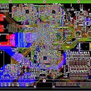
The first step is to get a piece of PCB, first in the paper to record all elements of the model, parameters, as well as the location, especially the diode, the direction of the triple tube, the direction of the IC gap.It is better to digital camera two pictures from a location.Now the PCB more do more advanced the diode triode, some do not pay attention to don’t see above.
The second step, tear down all laminated copy board, the tin in the PAD holes and be removed.PCB clean with alcohol, and then put into the scanner, the scanner to scan when need somewhat higher scan pixels, in order to get a clear image.Yarn paper will top and bottom with water slightly grinding, polishing to copper film, into the scanner, start PHOTOSHOP, knocked two layers respectively into in color mode.Note that the PCB must be horizontal even vertical, put in the scanner or scanning image is unusable.
The third step, adjust the contrast of the canvas, the contrast, the copper film part of and not part of the copper film contrast, then the first figure to black and white, check whether the line is clear, if not clear, repeat this step.If clear, will survive for the black and white TOP. The BMP file format of BMP and BOT. BMP, if found problems graphics can also repair and correction in PHOTOSHOP
The fourth step, the two BMP format into PROTEL format file, respectively in PROTEL transfer into two layers, such as a two layer of the PAD and the location of the VIA basic coincidence, that several steps before doing very well, if there is a deviation, then repeat step 3.So PCB copy board is a very need patience work, because a little problem will affect the quality and copy the board after the match.
Fifth, TOP. The TOP layer of BMP can be converted to PCB, be careful to into a SILK layer, the layer is yellow, then you are in the TOP layer is tracing, and drawing device according to the second step.After the draw will delete the SILK layer.Repeated know to draw all the layers.
Step 6, TOP in PROTEL PCB and BOT. PCB paged, into a graph with respect to OK.
Step 7, the TOPLAYER with laser printers, BOTTOMLAYER respectively printed on transparent film (1:1 ratio), put the film on the PCB, compare the errors, if yes, you’re done.
A and the original plate the same copy board was born, but it is only half done.Test, test copy plate electronic technology performance is same as the original plate.If it is completed. Note: if it is a multilayer and careful polishing to the lining of the inside, at the same time, repeat steps, the third to the fifth copy board graphic name is different, of course, want to be decided according to the number of layers, the general double panel is much simpler than a multilayer copy board, multilayer copy plate prone to alignment, so profes sional copy board look and careful (including internal guide hole and guide hole is not easy to appear problem).