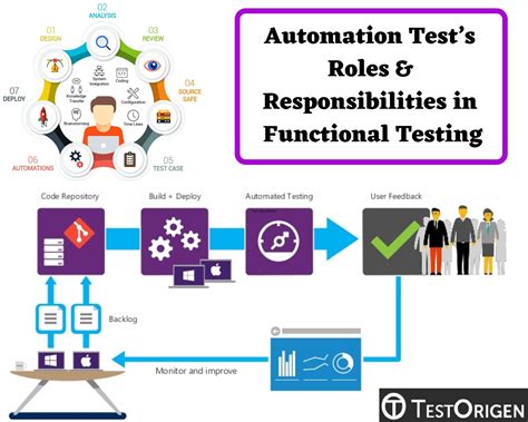
Introduction to Functional Testing
Functional testing is a crucial step in the PCB Assembly process that ensures the proper operation of the assembled printed circuit board (PCB). It involves testing the PCB’s functionality to verify that it meets the required specifications and performs as intended. Functional testing is performed after the PCB has been assembled and before it is shipped to the customer or integrated into a larger system.
Importance of Functional Testing in PCB Assembly
Functional testing is essential in PCB assembly for several reasons:
-
Quality Assurance: Functional testing helps to identify any defects or issues with the PCB’s functionality, ensuring that only high-quality and reliable PCBs are delivered to the customer.
-
Cost Reduction: By detecting defects early in the assembly process, functional testing can help to reduce the cost of rework and repairs, as well as minimize the risk of product recalls or field failures.
-
Customer Satisfaction: Functional testing ensures that the PCB meets the customer’s requirements and specifications, leading to higher customer satisfaction and loyalty.
-
Compliance: Functional testing helps to ensure that the PCB complies with industry standards and regulations, such as IPC (Association Connecting Electronics Industries) standards.
Types of Functional Testing
There are various types of functional testing that can be performed on a PCB, depending on the specific requirements and complexity of the board. Some common types of functional testing include:
In-Circuit Testing (ICT)
In-circuit testing is a type of functional testing that involves testing individual components on the PCB to ensure that they are properly connected and functioning as expected. ICT is typically performed using a bed-of-nails fixture, which makes contact with specific test points on the PCB.
| Advantages of ICT | Disadvantages of ICT |
|---|---|
| High fault coverage | Requires custom test fixtures |
| Fast test execution | Limited access to some components |
| Detects manufacturing defects | May not detect all functional issues |
Flying Probe Testing
Flying probe testing is a type of functional testing that uses movable probes to make contact with test points on the PCB. Unlike ICT, flying probe testing does not require a custom test fixture, making it more flexible and adaptable to different PCB designs.
| Advantages of Flying Probe Testing | Disadvantages of Flying Probe Testing |
|---|---|
| No custom test fixtures required | Slower test execution compared to ICT |
| Adaptable to different PCB designs | Higher cost per test |
| Can test both sides of the PCB | Limited test coverage for some components |
Boundary Scan Testing
Boundary scan testing, also known as JTAG (Joint Test Action Group) testing, is a type of functional testing that uses a special test access port (TAP) to test the interconnections between components on the PCB. Boundary scan testing is particularly useful for testing complex PCBs with high-density component packages.
| Advantages of Boundary Scan Testing | Disadvantages of Boundary Scan Testing |
|---|---|
| Tests interconnections between components | Requires components with JTAG support |
| Can test components not accessible by other methods | Limited test coverage for analog components |
| Useful for complex, high-density PCBs | Requires specialized software and hardware |
Functional Test Fixtures
Functional test fixtures are custom-designed fixtures that simulate the actual operating environment of the PCB. These fixtures allow for comprehensive testing of the PCB’s functionality, including power supply, input/output signals, and communication interfaces.
| Advantages of Functional Test Fixtures | Disadvantages of Functional Test Fixtures |
|---|---|
| Comprehensive testing of PCB functionality | Requires custom design and fabrication |
| Simulates actual operating environment | Higher cost compared to other test methods |
| Can test multiple aspects of PCB performance | Longer setup and testing time |

Functional Testing Process
The functional testing process typically involves the following steps:
-
Test Planning: Develop a comprehensive test plan that outlines the specific tests to be performed, test equipment required, and acceptance criteria.
-
Test Fixture Design: Design and fabricate custom test fixtures, if required, based on the PCB design and test requirements.
-
Test Program Development: Create test programs and scripts that automate the functional testing process and ensure consistent and repeatable results.
-
Test Execution: Perform the functional tests according to the test plan, using the appropriate test equipment and fixtures.
-
Results Analysis: Analyze the test results to identify any defects or issues with the PCB’s functionality and determine the root cause of the problems.
-
Rework and Retesting: Perform necessary rework and repairs on the PCB, and retest to ensure that the defects have been corrected and the PCB meets the required specifications.

Best Practices for Functional Testing
To ensure effective and efficient functional testing, consider the following best practices:
-
Early Involvement: Involve the test engineering team early in the PCB design process to ensure that the board is designed for testability and to identify potential test challenges.
-
Comprehensive Test Coverage: Develop a comprehensive test plan that covers all aspects of the PCB’s functionality, including power supply, input/output signals, communication interfaces, and environmental conditions.
-
Automated Testing: Use automated test equipment and software to improve test efficiency, consistency, and repeatability, and to reduce the risk of human error.
-
Continuous Improvement: Continuously monitor and analyze test results to identify opportunities for process improvement and optimization, and to reduce the risk of defects and failures.
-
Collaboration: Foster collaboration and communication between the design, manufacturing, and test engineering teams to ensure that all stakeholders are aligned and working towards common goals.

Frequently Asked Questions (FAQ)
-
What is the difference between functional testing and structural testing?
Functional testing focuses on verifying that the PCB performs its intended functions and meets the required specifications, while structural testing focuses on verifying the physical integrity and manufacturability of the PCB. -
Can functional testing detect all types of defects?
While functional testing is an effective method for detecting many types of defects, it may not detect all possible issues, such as intermittent or latent defects that may not manifest during the testing process. -
How long does functional testing typically take?
The duration of functional testing depends on the complexity of the PCB, the number of tests performed, and the test equipment and fixtures used. Typically, functional testing can take anywhere from a few minutes to several hours per board. -
What is the cost of functional testing?
The cost of functional testing varies depending on factors such as the complexity of the PCB, the test equipment and fixtures required, and the labor costs associated with test development and execution. However, the cost of functional testing is generally justified by the benefits of improved quality, reliability, and customer satisfaction. -
Can functional testing be outsourced?
Yes, functional testing can be outsourced to specialized test service providers or contract manufacturers with the necessary expertise, equipment, and facilities. Outsourcing functional testing can be a cost-effective option for companies that do not have the in-house resources or expertise to perform testing internally.
Conclusion
Functional testing is a critical step in the PCB assembly process that ensures the proper operation and reliability of the assembled board. By verifying that the PCB meets the required specifications and performs as intended, functional testing helps to improve quality, reduce costs, and enhance customer satisfaction.
There are various types of functional testing, including in-circuit testing, flying probe testing, boundary scan testing, and functional test fixtures, each with its own advantages and disadvantages. The choice of test method depends on factors such as the complexity of the PCB, the required test coverage, and the available resources and expertise.
To ensure effective and efficient functional testing, it is important to follow best practices such as early involvement of the test engineering team, comprehensive test coverage, automated testing, continuous improvement, and collaboration between stakeholders.
By investing in functional testing and making it an integral part of the PCB assembly process, companies can deliver high-quality, reliable products that meet customer expectations and drive business success.