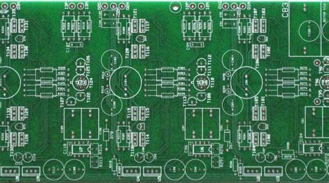
Introduction to PCB Duplication
Printed Circuit Boards (PCBs) are essential components in modern electronic devices, ranging from smartphones and computers to industrial equipment and medical devices. As technology advances and the demand for electronic products grows, the question arises: Can a PCB be copied? In this article, we will explore the concept of PCB duplication, its techniques, advantages, and challenges.
What is PCB Duplication?
PCB duplication is the process of creating an exact replica of an existing PCB design. This process involves analyzing the original PCB, extracting its design information, and reproducing it on a new board. PCB duplication can be performed for various reasons, such as:
- Reverse Engineering
- Obsolescence management
- Cost reduction
- Prototyping and testing
Techniques for PCB Duplication
There are several techniques used for PCB duplication, each with its own advantages and limitations. Let’s explore some of the most common methods:
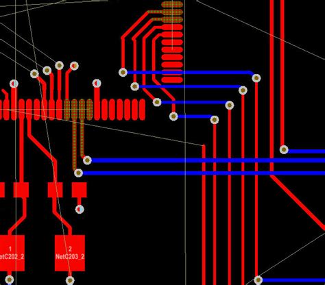
1. Visual Inspection and Manual Tracing
The simplest method of PCB duplication is through visual inspection and manual tracing. This technique involves carefully examining the original PCB and manually tracing its components, connections, and tracks onto a new board. While this method is cost-effective and requires minimal equipment, it is time-consuming and prone to human error, especially for complex designs.
2. X-Ray Imaging
X-ray imaging is a non-destructive technique used to capture the internal structure of a PCB. By using X-rays, engineers can visualize the layers, components, and connections within the board without damaging it. This method is particularly useful for multilayer PCBs and boards with hidden or buried vias. However, X-ray imaging requires specialized equipment and expertise, making it more expensive than manual tracing.
3. 3D Scanning
3D scanning is an advanced technique that utilizes specialized scanners to create a digital 3D model of the PCB. This method captures the board’s geometry, components, and connections with high accuracy. The resulting 3D model can be used for analysis, modification, and reproduction. 3D scanning is suitable for complex PCBs and provides a comprehensive understanding of the board’s structure. However, it requires expensive equipment and software, and the scanning process can be time-consuming.
4. Destructive Reverse Engineering
Destructive reverse engineering involves physically deconstructing the original PCB to analyze its internal structure and components. This method is used when non-destructive techniques are insufficient or when a detailed understanding of the board’s construction is required. Destructive reverse engineering is typically performed layer by layer, allowing engineers to examine each layer separately. While this method provides the most accurate information, it permanently destroys the original PCB and is not suitable for rare or expensive boards.
Advantages of PCB Duplication
PCB duplication offers several benefits, making it an attractive option for various applications. Some of the key advantages include:
1. Cost Reduction
By duplicating an existing PCB design, companies can save on research and development costs associated with creating a new design from scratch. This is particularly beneficial for projects with tight budgets or when the original design has proven to be reliable and efficient.
2. Time Savings
PCB duplication can significantly reduce the time required to bring a product to market. Instead of spending months or even years developing a new PCB design, engineers can duplicate an existing board and make necessary modifications, accelerating the development process.
3. Obsolescence Management
As electronic components become obsolete, finding replacements can be challenging and expensive. PCB duplication allows companies to recreate obsolete boards using modern components, extending the life of their products and reducing the need for costly redesigns.
4. Prototyping and Testing
PCB duplication is valuable for prototyping and testing purposes. By creating replicas of an existing design, engineers can experiment with modifications, test new components, and validate the board’s performance without risking damage to the original PCB.

Challenges in PCB Duplication
While PCB duplication offers numerous benefits, it also presents several challenges that must be considered:
1. Intellectual Property Concerns
PCB designs are often protected by intellectual property rights, such as patents and copyrights. Duplicating a PCB without proper authorization can lead to legal issues and potential lawsuits. It is crucial to ensure that the duplication process complies with relevant laws and regulations and that necessary permissions are obtained from the original design owner.
2. Component Availability
When duplicating an older PCB, finding the exact components used in the original design may be difficult. Some components may be obsolete or no longer in production, requiring engineers to find suitable replacements or redesign certain aspects of the board.
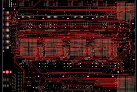
3. Design Complexity
Complex PCB designs, such as those with multiple layers, fine pitch components, or high-density interconnects, can be challenging to duplicate accurately. The duplication process requires precise measurements, advanced equipment, and skilled engineers to ensure the replicated board functions as intended.
4. Quality Assurance
Ensuring the quality and reliability of a duplicated PCB is critical. The replicated board must undergo thorough testing and validation to verify that it meets the same performance standards as the original design. This process can be time-consuming and requires access to specialized testing equipment and expertise.
FAQs
-
Q: Is PCB duplication legal?
A: PCB duplication is legal when performed with the proper authorization and in compliance with intellectual property laws and regulations. It is essential to obtain permission from the original design owner before duplicating a PCB. -
Q: How accurate is PCB duplication?
A: The accuracy of PCB duplication depends on the technique used and the complexity of the original design. Advanced methods like 3D scanning and destructive reverse engineering can provide highly accurate results, while manual tracing is more prone to errors. -
Q: Can PCB duplication be used for mass production?
A: Yes, PCB duplication can be used for mass production once the replicated design has been thoroughly tested and validated. However, it is essential to ensure that the duplicated design meets all necessary performance and quality standards before proceeding with mass production. -
Q: How much does PCB duplication cost?
A: The cost of PCB duplication varies depending on the complexity of the design, the technique used, and the required resources. Simple designs duplicated using manual tracing may be relatively inexpensive, while complex designs requiring advanced techniques like 3D scanning or destructive reverse engineering can be more costly. -
Q: How long does PCB duplication take?
A: The time required for PCB duplication depends on the complexity of the design, the chosen duplication technique, and the availability of resources. Simple designs duplicated using manual tracing can be completed in a few days, while complex designs requiring advanced techniques may take several weeks or even months.
Conclusion
PCB duplication is a valuable process that allows engineers to create exact replicas of existing PCB designs. By leveraging techniques such as visual inspection, X-ray imaging, 3D scanning, and destructive reverse engineering, companies can reduce costs, save time, manage obsolescence, and streamline prototyping and testing. However, PCB duplication also presents challenges, such as intellectual property concerns, component availability, design complexity, and quality assurance.
As technology continues to advance, the demand for PCB duplication is likely to grow. By understanding the techniques, advantages, and challenges involved in PCB duplication, engineers and companies can make informed decisions and leverage this process to create innovative and reliable electronic products.
| Technique | Advantages | Limitations |
|---|---|---|
| Visual Inspection & Manual Tracing | – Cost-effective – Minimal equipment required |
– Time-consuming – Prone to human error – Limited complexity |
| X-Ray Imaging | – Non-destructive – Suitable for multilayer PCBs |
– Expensive equipment – Requires expertise |
| 3D Scanning | – High accuracy – Comprehensive 3D model – Suitable for complex PCBs |
– Expensive equipment and software – Time-consuming process |
| Destructive Reverse Engineering | – Most accurate information – Detailed layer-by-layer analysis |
– Permanently destroys the original PCB – Not suitable for rare or expensive boards |
By carefully considering the available techniques and weighing the advantages and limitations of each, engineers can select the most appropriate method for their specific PCB duplication needs. With the right approach and expertise, PCB duplication can be a powerful tool for driving innovation and success in the electronics industry.