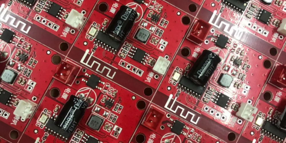
The different processes of circuit boards are described in detail as follows:
1、Single panel process flow
Under the material grinding edge → drilling → outer layer graphics → (full board gold plating) → etching → inspection → screen printing solder resistance → (hot air leveling) → screen printing characters → shape processing → test → inspection.
2、Double-sided nickel-gold plating process
Under the material grinding edge → drilling → sinking copper thickening → outer layer graphics → nickel plating, gold de-film etching → secondary drilling → inspection → screen printing resistance welding → screen printing characters → shape processing → test → inspection.
3、Tin spraying plate process for double-sided panel
Material grinding→drilling→sinking copper thickening→the outer layer of graphics→tinning, etching retinning→secondary drilling→inspection→screen printing soldering→gold plating plug→hot air leveling→screen printing characters→shape processing→testing→inspection.
4、Nickel and gold plating process of multilayer board
Edge grinding → drilling positioning holes → inner layer graphics → inner layer etching → inspection → blackening → lamination → drilling → copper thickening → outer layer graphics → gold plating, de-film etching → secondary drilling → inspection → silk-screening resist welding → silk-screening characters → shape processing → test → inspection.
5、Tin spraying process of multilayer board
Grind the edge of the material → drill the positioning hole → inner layer graphics → inner layer etching → inspection → blackening → lamination → drilling → sink copper thickening → outer layer graphics → tin plating, etching retinning → secondary drilling → inspection → silk-screening resistance welding → gold-plated plug → hot air leveling → silk-screening characters → shape processing → test → inspection.
6、Sink nickel gold plate process of multilayer board
Edge grinding → drilling positioning holes → inner layer graphics → inner layer etching → inspection → blackening → lamination → drilling → sinking copper thickening → outer layer graphics → tin plating, etching retinning → secondary drilling → inspection → silk-screening resist soldering → chemically sunk nickel gold → silk-screening characters → shape processing → test → inspection.
