Mistake 1: Inadequate Planning and Documentation
One of the most significant mistakes in PCB design is failing to plan and document the design process adequately. Before starting the design, it is essential to gather all the necessary information, such as the schematic diagram, bill of materials (BOM), and mechanical constraints. This information should be reviewed and verified to ensure that it is accurate and complete.
Importance of Planning and Documentation
Proper planning and documentation can help avoid delays, errors, and unnecessary iterations in the design process. It also ensures that all stakeholders, including the design team, manufacturing team, and customers, are on the same page regarding the project requirements and expectations.
Best Practices for Planning and Documentation
- Create a detailed project plan that outlines the design process, timeline, and deliverables.
- Use a version control system to track changes and revisions to the design files.
- Maintain a clear and concise design document that includes the schematic diagram, BOM, layout guidelines, and manufacturing requirements.
- Conduct regular design reviews with the team to identify and address any issues or concerns.
| Document | Purpose |
|---|---|
| Project Plan | Outlines the design process, timeline, and deliverables |
| Schematic Diagram | Shows the electrical connections between components |
| Bill of Materials (BOM) | Lists all the components used in the design |
| Layout Guidelines | Specifies the design rules and constraints for the PCB layout |
| Manufacturing Requirements | Defines the manufacturing process and specifications |
Mistake 2: Ignoring Design for Manufacturability (DFM)
Another common mistake in PCB design is ignoring the principles of Design for Manufacturability (DFM). DFM is the practice of designing products that are easy to manufacture, assemble, and test. Ignoring DFM can lead to manufacturing issues, such as poor yield, high defect rates, and increased production costs.
Importance of DFM
Designing for manufacturability can help reduce production costs, improve product quality, and shorten time-to-market. It also ensures that the PCB can be manufactured consistently and reliably, reducing the risk of product failures and warranty claims.
Best Practices for DFM
- Follow the manufacturer’s design guidelines and specifications.
- Use standard component sizes and packages whenever possible.
- Provide adequate clearances and spacing between components and traces.
- Avoid using fine pitch components or small vias that are difficult to manufacture.
- Use a panelization strategy that optimizes the use of the PCB material and minimizes waste.
| Parameter | Recommended Value |
|---|---|
| Minimum Trace Width | 0.2 mm |
| Minimum Trace Spacing | 0.2 mm |
| Minimum Drill Size | 0.3 mm |
| Minimum Annular Ring | 0.15 mm |
| Minimum Solder Mask Opening | 0.1 mm |

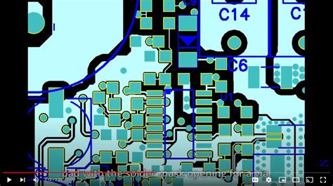
Mistake 3: Poor Component Placement and Routing
Component placement and routing are critical aspects of PCB design that can impact the performance, reliability, and manufacturability of the product. Poor component placement and routing can lead to signal integrity issues, electromagnetic interference (EMI), and thermal problems.
Importance of Component Placement and Routing
Proper component placement and routing can help optimize the PCB layout, reduce the board size, and improve the overall performance of the product. It also ensures that the PCB can be manufactured efficiently and reliably, reducing the risk of defects and failures.
Best Practices for Component Placement and Routing
- Place components logically and functionally, grouping related components together.
- Minimize the distance between components to reduce the trace length and improve signal integrity.
- Use a grid-based placement strategy to ensure proper alignment and spacing between components.
- Route critical signals first, such as power, ground, and high-speed signals.
- Use a star grounding scheme to minimize ground loops and reduce EMI.
- Avoid crossing traces and vias whenever possible to reduce signal coupling and crosstalk.
| Signal Type | Routing Strategy |
|---|---|
| Power | Use wide traces and multiple vias to minimize voltage drop and improve current carrying capacity |
| Ground | Use a solid ground plane and multiple vias to minimize ground bounce and EMI |
| High-Speed | Use controlled impedance traces and avoid sharp bends or vias to minimize signal reflections and distortions |
| Analog | Separate analog and digital signals and use guard traces to minimize crosstalk and noise coupling |

Mistake 4: Neglecting Signal Integrity and EMC
Signal integrity and electromagnetic compatibility (EMC) are critical aspects of PCB design that can impact the performance, reliability, and safety of the product. Neglecting signal integrity and EMC can lead to signal distortion, crosstalk, EMI, and even product failures.
Importance of Signal Integrity and EMC
Ensuring signal integrity and EMC can help improve the performance and reliability of the product, reduce the risk of interference with other electronic devices, and meet regulatory requirements for electromagnetic emissions and susceptibility.
Best Practices for Signal Integrity and EMC
- Use controlled impedance traces for high-speed signals to minimize reflections and distortions.
- Terminate high-speed signals properly using resistors or other termination devices.
- Use differential signaling for high-speed interfaces to minimize EMI and improve noise immunity.
- Provide adequate shielding and grounding for sensitive components and signals.
- Follow EMC design guidelines and conduct EMC testing to ensure compliance with regulatory standards.
| Parameter | Recommended Value |
|---|---|
| Trace Impedance | 50 ohms for single-ended signals, 100 ohms for differential signals |
| Termination Resistor | Matched to the trace impedance |
| Via Stub Length | Less than 1/4 of the signal wavelength |
| Decoupling Capacitor | Placed close to the power pins of ICs |
| Shielding | Use conductive enclosures and gaskets for sensitive components |

Mistake 5: Insufficient Testing and Verification
Finally, insufficient testing and verification is a common mistake in PCB design that can lead to product failures, delays, and increased costs. Testing and verification should be an integral part of the design process, from the schematic level to the final manufactured product.
Importance of Testing and Verification
Thorough testing and verification can help identify and correct design errors early in the process, reducing the risk of costly redesigns and production delays. It also ensures that the product meets the performance, reliability, and safety requirements, reducing the risk of product failures and recalls.
Best Practices for Testing and Verification
- Conduct schematic-level simulations to verify the electrical functionality of the design.
- Perform layout-level simulations to analyze signal integrity, EMC, and thermal performance.
- Use automated design rule checks (DRC) and electrical rule checks (ERC) to verify the design against the manufacturing and electrical constraints.
- Conduct prototype testing to validate the design and identify any issues or improvements.
- Perform final testing and inspection on the manufactured product to ensure conformance to specifications.
| Test | Purpose |
|---|---|
| Schematic Simulation | Verifies the electrical functionality of the design |
| Layout Simulation | Analyzes signal integrity, EMC, and thermal performance |
| Design Rule Check (DRC) | Verifies the design against manufacturing constraints |
| Electrical Rule Check (ERC) | Verifies the design against electrical constraints |
| Prototype Testing | Validates the design and identifies any issues or improvements |
| Final Testing and Inspection | Ensures conformance to specifications |
Frequently Asked Questions (FAQ)
-
What is the most important aspect of PCB design?
The most important aspect of PCB design is ensuring the functionality, reliability, and manufacturability of the product. This requires a holistic approach that considers all aspects of the design, from the schematic to the final manufactured product. -
How can I improve the signal integrity of my PCB design?
To improve the signal integrity of your PCB design, you can use controlled impedance traces, terminate high-speed signals properly, use differential signaling, and provide adequate shielding and grounding for sensitive components and signals. -
What is Design for Manufacturability (DFM) and why is it important?
Design for Manufacturability (DFM) is the practice of designing products that are easy to manufacture, assemble, and test. It is important because it can help reduce production costs, improve product quality, and shorten time-to-market. -
How can I avoid EMI issues in my PCB design?
To avoid EMI issues in your PCB design, you can use a solid ground plane, provide adequate shielding for sensitive components, use differential signaling for high-speed interfaces, and follow EMC design guidelines and conduct EMC testing to ensure compliance with regulatory standards. -
What are the benefits of thorough testing and verification in PCB design?
Thorough testing and verification in PCB design can help identify and correct design errors early in the process, reducing the risk of costly redesigns and production delays. It also ensures that the product meets the performance, reliability, and safety requirements, reducing the risk of product failures and recalls.
Conclusion
PCB design is a complex process that requires attention to detail, planning, and careful consideration of all aspects of the design. By avoiding these five common mistakes – inadequate planning and documentation, ignoring DFM, poor component placement and routing, neglecting signal integrity and EMC, and insufficient testing and verification – you can improve the quality, reliability, and manufacturability of your PCB designs. Remember to follow best practices, use appropriate tools and techniques, and collaborate with your team and stakeholders to ensure a successful outcome.