The History of Printed Circuit Boards
The concept of printed circuit boards can be traced back to the early 20th century. In 1903, Albert Hanson, a German inventor, filed a patent for a method of creating conductive patterns on an insulating material. However, it wasn’t until the 1940s that printed circuit boards began to gain widespread use in the electronics industry.
During World War II, the demand for compact and reliable electronic equipment increased significantly. In 1943, Paul Eisler, an Austrian engineer, developed a process for printing conductive ink onto a non-conductive substrate, which became the foundation for modern PCB manufacturing.
In the 1950s, the U.S. military adopted printed circuit boards for use in their electronic equipment, which further accelerated the development and adoption of PCB technology. By the 1960s, PCBs had become the standard method for assembling electronic circuits in both military and consumer applications.
The Manufacturing Process of PCBs
The manufacturing process of printed circuit boards involves several steps, each of which is critical to ensuring the quality and reliability of the final product. The main steps in PCB manufacturing are as follows:
-
Design: The first step in creating a PCB is to design the circuit using specialized software, such as Eagle or KiCad. The design includes the placement of components, routing of conductive traces, and the creation of solder masks and silkscreen layers.
-
Printing: Once the design is complete, the PCB layout is printed onto a transparent film or photomask. This film is used to transfer the circuit pattern onto the copper-clad board during the etching process.
-
Etching: The copper-clad board is coated with a light-sensitive resist material and then exposed to UV light through the photomask. The areas of the resist that are exposed to light harden, while the unexposed areas remain soluble. The board is then placed in an etching solution, which removes the unprotected copper, leaving behind the desired conductive traces.
-
Drilling: After etching, holes are drilled into the board to accommodate through-hole components and to create vias, which are used to connect traces on different layers of the board.
-
Plating: The drilled holes are then plated with copper to ensure a reliable electrical connection between layers. Additional plating, such as tin-lead or gold, may be applied to improve solderability and prevent oxidation.
-
Solder Mask and Silkscreen: A solder mask, typically green in color, is applied to the board to protect the copper traces from accidental short-circuits during soldering. A silkscreen layer, which contains text and symbols, is then added to help identify components and provide assembly instructions.
-
Surface Mount Assembly: Surface mount components are placed onto the board using a pick-and-place machine, which uses computer vision to accurately position the components on the designated pads. The board is then run through a reflow oven, which melts the solder paste and permanently attaches the components to the board.
-
Through-Hole Assembly: For through-hole components, the leads are inserted into the drilled holes, and the board is then sent through a wave soldering machine, which applies molten solder to the underside of the board, creating a connection between the component leads and the copper traces.
-
Inspection and Testing: After assembly, the PCB undergoes various inspections and tests to ensure proper functionality and adherence to quality standards. This may include visual inspections, automated optical inspections (AOI), X-ray inspections, and electrical testing.
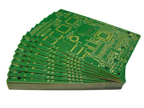
Types of Printed Circuit Boards
There are several types of printed circuit boards, each with its own unique characteristics and applications. The most common types of PCBs are:
-
Single-Sided PCBs: These boards have conductive traces on only one side of the insulating substrate. Single-sided PCBs are the simplest and most cost-effective option, making them suitable for low-complexity circuits and prototypes.
-
Double-Sided PCBs: As the name suggests, double-sided PCBs have conductive traces on both sides of the insulating substrate. The two sides are connected using through-hole vias, allowing for more complex circuits and higher component density compared to single-sided boards.
-
Multi-Layer PCBs: These boards consist of multiple layers of insulating material and conductive traces, sandwiched together to form a single board. Multi-layer PCBs can have anywhere from four to over thirty layers, allowing for extremely complex circuits and high component density. They are commonly used in advanced electronic devices, such as smartphones, computers, and medical equipment.
-
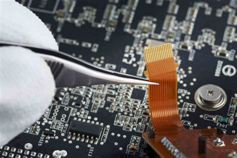
Flexible PCBs: Flexible PCBs are made using a flexible insulating material, such as polyimide, which allows the board to bend and conform to various shapes. They are often used in applications where space is limited or where the board needs to fit into a specific form factor, such as in wearable devices or automotive electronics.
-
Rigid-Flex PCBs: Rigid-flex PCBs combine the benefits of both rigid and flexible boards. They consist of rigid sections, which provide structural support and house most of the components, and flexible sections, which allow the board to bend and fold as needed. Rigid-flex PCBs are commonly used in aerospace, military, and medical applications.

Advantages of Using Printed Circuit Boards
Printed circuit boards offer numerous advantages over other methods of assembling electronic circuits, such as point-to-point wiring or wire-wrap. Some of the key benefits of using PCBs include:
-
Consistency and Reliability: PCBs are manufactured using automated processes, which ensures a high degree of consistency and reliability between boards. This reduces the risk of errors and improves the overall quality of the final product.
-
Compact Size: By using PCBs, electronic circuits can be made much smaller and more compact than with other assembly methods. This is particularly important in modern electronic devices, where space is often at a premium.
-
Reduced Assembly Time: PCBs allow for automated assembly processes, such as pick-and-place and reflow soldering, which significantly reduces the time required to assemble a complete circuit. This can lead to faster production times and lower manufacturing costs.
-
Improved Signal Integrity: The precise layout and routing of conductive traces on a PCB help to minimize signal interference and crosstalk, which is essential for high-speed and high-frequency applications.
-
Easier Maintenance and Repair: PCBs make it easier to identify and replace faulty components, as each component has a designated location on the board. This can simplify maintenance and repair tasks, reducing downtime and associated costs.
Applications of Printed Circuit Boards
Printed circuit boards are used in virtually every electronic device, from simple consumer gadgets to complex industrial equipment. Some of the most common applications of PCBs include:
-
Consumer Electronics: PCBs are found in a wide range of consumer devices, such as smartphones, tablets, laptops, televisions, gaming consoles, and home appliances.
-
Automotive Electronics: Modern vehicles rely heavily on electronic systems for various functions, such as engine management, infotainment, and advanced driver assistance systems (ADAS). PCBs are essential components in these systems, providing reliable and compact solutions for automotive applications.
-
Medical Devices: PCBs are used in numerous medical devices, including patient monitors, imaging equipment, and implantable devices such as pacemakers and defibrillators. In these applications, PCBs must meet stringent quality and reliability standards to ensure patient safety.
-
Industrial Equipment: PCBs are used in a variety of industrial applications, such as process control systems, automation equipment, and power electronics. In these environments, PCBs must be designed to withstand harsh conditions, such as extreme temperatures, vibration, and exposure to chemicals.
-
Aerospace and Defense: PCBs are critical components in aerospace and defense applications, where reliability and performance are paramount. Examples include avionics systems, radar equipment, and satellite communications hardware.
PCB design Considerations
Designing a printed circuit board involves several key considerations to ensure optimal performance, reliability, and manufacturability. Some of the most important aspects of PCB design include:
-
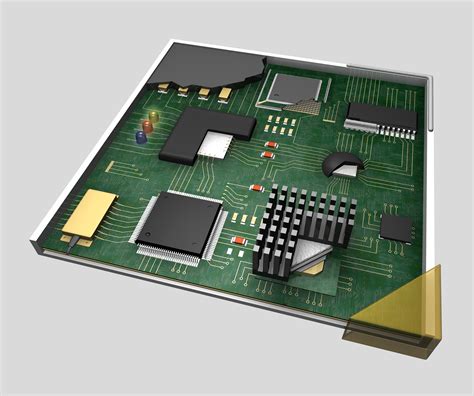
Component Placement: The placement of components on a PCB can have a significant impact on signal integrity, thermal management, and manufacturability. Designers must consider factors such as component size, pin spacing, and heat dissipation when determining the optimal placement.
-
Trace Routing: The routing of conductive traces on a PCB is critical for ensuring proper signal integrity and minimizing interference. Designers must consider factors such as trace width, spacing, and impedance when routing traces, particularly for high-speed or high-frequency signals.
-
Grounding and Shielding: Proper grounding and shielding techniques are essential for minimizing electromagnetic interference (EMI) and ensuring stable operation. This may involve the use of ground planes, shielding layers, and careful placement of sensitive components.
-
Thermal Management: Managing heat dissipation is crucial for ensuring the long-term reliability of a PCB and its components. Designers must consider factors such as component power ratings, ambient temperatures, and available cooling methods when designing for thermal management.
-
Manufacturing Constraints: PCB designers must also consider the limitations and capabilities of the manufacturing process when creating their designs. This includes factors such as minimum trace widths, hole sizes, and clearances, as well as the availability of specific materials or surface finishes.
Frequently Asked Questions (FAQ)
- What is the difference between a PCB and a printed wiring board (PWB)?
-
A printed wiring board (PWB) is a more general term that includes both printed circuit boards (PCBs) and other types of boards that use conductive traces for interconnections. In practice, however, the terms PCB and PWB are often used interchangeably.
-
What materials are used to make PCBs?
-
The most common base material for PCBs is FR-4, which is a composite material made from woven fiberglass and epoxy resin. Other materials, such as polyimide, ceramic, and metal-core substrates, may be used for specific applications or environments.
-
How are PCBs tested for quality and reliability?
-
PCBs undergo various tests to ensure quality and reliability, including visual inspections, automated optical inspections (AOI), X-ray inspections, and electrical tests such as continuity, insulation resistance, and high-potential (hipot) testing. Environmental stress tests, such as thermal cycling and humidity exposure, may also be performed to validate the board’s performance under specific conditions.
-
What is the typical turnaround time for PCB manufacturing?
-
The turnaround time for PCB manufacturing varies depending on factors such as board complexity, layer count, and the manufacturer’s capacity. Simple, single-sided boards may be produced in as little as 24 hours, while complex, multi-layer boards may take several weeks. Most PCB manufacturers offer standard lead times of 5-15 business days for typical orders.
-
How can I ensure my PCB design is ready for manufacturing?
- To ensure your PCB design is ready for manufacturing, you should work closely with your chosen PCB manufacturer and adhere to their design guidelines. This includes factors such as minimum trace widths, hole sizes, and clearances, as well as the use of appropriate design file formats (e.g., Gerber, ODB++). Many PCB manufacturers offer design review services to help identify and address potential issues before production begins.
| PCB Type | Layers | Typical Applications |
|---|---|---|
| Single-Sided | 1 | Simple circuits, prototypes, low-cost products |
| Double-Sided | 2 | Moderately complex circuits, consumer electronics |
| Multi-Layer | 4+ | Complex circuits, high-density designs, advanced electronics |
| Flexible | 1+ | Wearables, automotive, aerospace, medical devices |
| Rigid-Flex | 2+ | Aerospace, military, medical devices, high-reliability applications |
In conclusion, printed circuit boards (PCBs) are essential components in modern electronics, providing a reliable and efficient means of interconnecting electronic components. From their early beginnings in the 20th century to their widespread use today, PCBs have enabled the development of increasingly complex and compact electronic devices across a wide range of industries and applications.
As technology continues to advance, the design and manufacturing of PCBs will play a crucial role in shaping the future of electronics, enabling new innovations and pushing the boundaries of what is possible.