What is AutoCAD?
AutoCAD is a commercial CAD software developed by Autodesk. It allows users to create, modify, and document 2D and 3D designs with high precision. AutoCAD offers a wide range of tools and features, making it suitable for various design tasks across different industries.
Key features of AutoCAD include:
- Precise 2D and 3D modeling
- Customizable user interface
- Extensive library of symbols and components
- Support for multiple file formats
- Collaboration tools for teamwork
PCB Design Requirements
Before discussing the use of AutoCAD for PCB design, let’s briefly review the key requirements for a PCB design software:
- Schematic capture: The ability to create and edit electronic schematics
- Component libraries: Access to a wide range of electronic component symbols and footprints
- PCB layout: Tools for placing components and routing traces on a PCB
- Design rule checking (DRC): Automated checks to ensure the PCB design meets manufacturing requirements
- Output generation: The ability to generate manufacturing files, such as Gerber and drill files

Using AutoCAD for PCB Design
Schematic Capture
AutoCAD does not have built-in tools for creating electronic schematics. However, it is possible to create schematic-like drawings using AutoCAD’s drawing and annotation tools. Users can create custom symbols for electronic components and use lines and polylines to represent connections between them.
While this approach may work for simple circuits, it lacks the specialized features found in dedicated schematic capture software, such as:
- Electrical rule checking (ERC)
- Netlist generation
- Bill of materials (BOM) creation
Component Libraries
AutoCAD does not come with a built-in library of electronic components. Users must create their own symbols and footprints or import them from external sources. This can be time-consuming and may not provide the same level of accuracy and consistency as the libraries found in dedicated PCB design software.
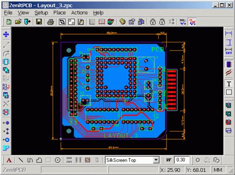
PCB Layout
AutoCAD’s precise drawing tools can be used to create PCB layouts. Users can draw the board outline, place component footprints, and route traces using lines and polylines. However, AutoCAD lacks several key features that are essential for efficient and accurate PCB layout, such as:
- Automatic component placement
- Interactive routing with design rule checks
- Copper pour and plane creation
- Multilayer support
Design Rule Checking (DRC)
AutoCAD does not have built-in design rule checking capabilities for PCB design. Users must manually verify that their designs meet manufacturing requirements, such as minimum trace width, clearance, and drill sizes. This process is prone to human error and can be time-consuming, especially for complex designs.
Output Generation
AutoCAD can export designs in various file formats, including DXF and DWG. However, it does not have the ability to generate the specific manufacturing files required for PCB fabrication, such as Gerber and drill files. Users must either manually create these files or use third-party software to convert their AutoCAD designs into the required formats.

Comparison with Dedicated PCB Design Software
To better understand the limitations of using AutoCAD for PCB design, let’s compare it with dedicated PCB design software:
| Feature | AutoCAD | Dedicated PCB software |
|---|---|---|
| Schematic Capture | Manual drawing, no ERC or netlist generation | Built-in schematic editor with ERC and netlist generation |
| Component Libraries | No built-in libraries, users must create or import | Extensive libraries of symbols and footprints |
| PCB Layout | Manual placement and routing, no DRC | Automatic placement, interactive routing with DRC |
| Design Rule Checking | No built-in DRC | Automated DRC for manufacturing requirements |
| Output Generation | No direct Gerber or drill file output | Generates Gerber, drill, and other manufacturing files |
As evident from the comparison, dedicated PCB design software offers a range of specialized features that simplify and automate the PCB design process. These features help ensure the accuracy, reliability, and manufacturability of the final design.
Alternatives to AutoCAD for PCB Design
If you are considering using AutoCAD for PCB design, it is worth exploring dedicated PCB design software alternatives. Some popular options include:
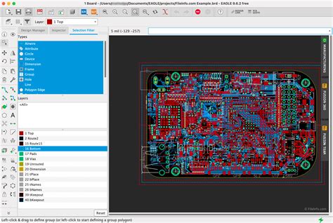
- Autodesk Eagle: A powerful PCB design software with schematic capture, component libraries, and automated routing
- KiCad: A free and open-source PCB design software with a full suite of tools for schematic capture, PCB layout, and manufacturing file generation
- Altium Designer: A professional-grade PCB design software with advanced features for high-speed and high-density designs
- OrCAD: A comprehensive PCB design solution with schematic capture, simulation, and layout capabilities
These dedicated PCB design software packages offer a more streamlined and efficient workflow for creating electronic designs, ensuring better results and faster turnaround times.
Frequently Asked Questions
1. Can I use AutoCAD to create PCB layouts?
While it is possible to use AutoCAD’s drawing tools to create PCB layouts, it is not the most efficient or reliable method. AutoCAD lacks specialized features for component placement, routing, and design rule checking, which can lead to errors and longer design times.
2. Are there any advantages to using AutoCAD for PCB design?
The main advantage of using AutoCAD for PCB design is familiarity. If you are already proficient in AutoCAD, you may find it easier to adapt your skills to PCB design. However, the lack of specialized features and automation can make the process more challenging and time-consuming compared to using dedicated PCB design software.
3. Can I convert my AutoCAD PCB designs to manufacturing files?
AutoCAD does not have built-in capabilities to generate manufacturing files, such as Gerber and drill files. You would need to use third-party software to convert your AutoCAD designs into the required formats, which can introduce compatibility issues and additional steps in the design process.
4. What are the risks of using AutoCAD for PCB design?
Using AutoCAD for PCB design can result in several risks, including:
- Increased likelihood of design errors due to the lack of automated checks and rule enforcement
- Longer design times due to manual placement, routing, and verification processes
- Potential issues with manufacturing due to the lack of direct output generation for required files
5. Should I learn AutoCAD for PCB design or invest in dedicated software?
If your primary goal is to design PCBs efficiently and accurately, it is recommended to invest in learning and using dedicated PCB design software. These specialized tools offer a range of features and automation that simplify the design process, reduce errors, and ensure manufacturing compatibility.
Conclusion
While AutoCAD is a powerful and versatile CAD software, it is not the most suitable choice for PCB design. The lack of specialized features for schematic capture, component libraries, PCB layout, design rule checking, and manufacturing file generation can make the process more challenging and time-consuming compared to using dedicated PCB design software.
If you are serious about PCB design, it is recommended to explore and invest in specialized PCB design software, such as Autodesk Eagle, KiCad, Altium Designer, or OrCAD. These tools offer a more streamlined and efficient workflow, ensuring better results and faster turnaround times for your electronic design projects.