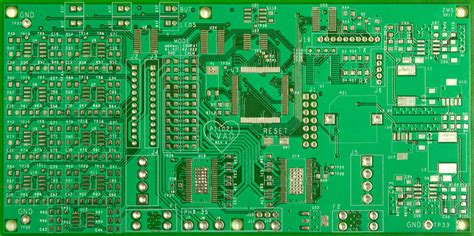
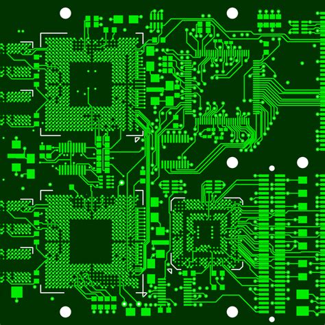
What is PCB design?
PCB design is the process of creating a layout for the electronic components and connections that will be etched onto a Printed Circuit Board. The design process involves several steps, including:
- Schematic capture: Creating a diagram of the electronic components and their connections.
- Component placement: Arranging the components on the board for optimal performance and manufacturability.
- Routing: Creating the copper traces that connect the components.
- Design rule checking: Verifying that the design meets all the necessary specifications and standards.
The Importance of PCB Design
PCB design is essential for creating reliable, efficient, and cost-effective electronic devices. A well-designed PCB can:
- Minimize signal interference and crosstalk
- Reduce electromagnetic interference (EMI)
- Improve power distribution and heat dissipation
- Enhance manufacturing efficiency and yield
PCB design software
To create a PCB design, engineers and designers use specialized software tools. Some of the most popular PCB design software packages include:
| Software | Company | Features |
|---|---|---|
| Altium Designer | Altium | 3D modeling, simulation, version control |
| OrCAD | Cadence | Schematic capture, simulation, autorouting |
| Eagle | Autodesk | Schematic capture, layout, autorouting |
| KiCad | Open Source | Schematic capture, layout, 3D viewer |
These software tools provide a range of features and capabilities to help designers create high-quality PCB layouts. They typically include schematic capture tools, component libraries, layout editors, and design rule checking tools.
The PCB Design Process
The PCB design process typically involves several stages, each with its own set of challenges and considerations.
Schematic Capture
The first step in PCB design is to create a schematic diagram of the electronic circuit. This involves selecting the appropriate components, such as resistors, capacitors, and integrated circuits, and defining their connections.
Schematic capture software tools allow designers to create these diagrams using a graphical interface, with pre-defined symbols for common components. The software also performs basic error checking, such as ensuring that all connections are complete and that there are no short circuits.
Component Placement
Once the schematic is complete, the next step is to place the components on the PCB layout. This involves considering factors such as:
- Component size and shape
- Pin spacing and orientation
- Power and ground connections
- Signal integrity and crosstalk
- Manufacturing constraints, such as minimum trace width and spacing
PCB design software tools provide automated placement tools that can help optimize the layout based on these factors. However, manual placement is often necessary to fine-tune the layout and ensure the best possible performance.
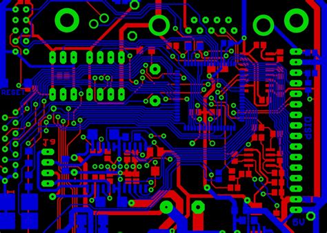
Routing
After the components are placed, the next step is to route the copper traces that connect them. This involves creating a network of traces on the various layers of the PCB, while avoiding obstacles such as vias, mounting holes, and other components.
PCB design software tools provide autorouting capabilities that can automatically generate trace routes based on predefined rules and constraints. However, manual routing is often necessary to optimize the layout for signal integrity, EMI reduction, and manufacturing efficiency.
Design Rule Checking
Throughout the PCB design process, it is important to ensure that the design meets all the necessary specifications and standards. This includes factors such as:
- Minimum trace width and spacing
- Drill hole size and spacing
- Solder mask and silkscreen requirements
- Electrical characteristics, such as impedance and capacitance
PCB design software tools provide design rule checking (DRC) tools that can automatically verify the design against a set of predefined rules. This helps catch errors and potential problems early in the design process, reducing the risk of costly manufacturing defects.
Manufacturing Considerations
Once the PCB design is complete, it must be manufactured using a variety of processes, including:
- Etching: Removing unwanted copper from the board to create the traces and pads
- Drilling: Creating holes for through-hole components and vias
- Plating: Adding additional copper or other metals to the holes and surfaces
- Solder mask: Applying a protective coating over the copper traces
- Silkscreen: Adding text and graphics to the board for identification and assembly
The PCB design must take these manufacturing processes into account, ensuring that the board can be efficiently and reliably produced. This includes factors such as:
- Minimum trace width and spacing for etching
- Drill hole size and spacing for drilling
- Clearance and creepage distances for high-voltage applications
- Solder mask and silkscreen tolerances

PCB Design Best Practices
To create high-quality PCB designs, engineers and designers should follow a set of best practices and guidelines. Some of these include:
Keep it Simple
Whenever possible, keep the PCB design as simple as possible. This means using the minimum number of layers, components, and connections necessary to achieve the desired functionality. A simpler design is easier to manufacture, test, and debug, and is less likely to have problems with signal integrity or EMI.
Use a Grid
When placing components and routing traces, use a grid to ensure consistent spacing and alignment. This helps improve the manufacturability of the board and reduces the risk of errors or defects.
Minimize Crosstalk
Crosstalk occurs when signals from one trace interfere with signals on adjacent traces. To minimize crosstalk, keep high-speed signals away from each other and use ground planes or guard traces to provide shielding.
Optimize Power Distribution
Proper power distribution is critical for ensuring reliable operation and minimizing noise and EMI. Use wide traces or planes for power and ground, and place decoupling capacitors close to high-speed components to reduce power supply noise.
Consider Thermal Management
As electronic devices become more powerful and compact, thermal management becomes increasingly important. Consider factors such as component placement, airflow, and heat sinking to ensure that the PCB can dissipate heat effectively.
Use Version Control
PCB design is an iterative process, with frequent revisions and updates. Use version control software to track changes and collaborate with other team members. This helps ensure that everyone is working with the most up-to-date version of the design and reduces the risk of errors or conflicts.
FAQ
What is the difference between a PCB and a breadboard?
A breadboard is a prototyping tool used to temporarily connect electronic components for testing and experimentation. It consists of a grid of holes that components can be plugged into, with interconnected rows and columns for easy wiring. A PCB, on the other hand, is a permanent printed circuit board that is used to interconnect electronic components in a final product.
What is the difference between through-hole and surface-mount components?
Through-hole components have leads that are inserted through holes in the PCB and soldered on the opposite side. Surface-mount components are mounted directly on the surface of the PCB, with small metal pads for soldering. Surface-mount components are smaller and more compact than through-hole components, but can be more difficult to work with manually.
What is the difference between a single-sided and double-sided PCB?
A single-sided PCB has copper traces and components on only one side of the board, while a double-sided PCB has copper traces and components on both sides. Double-sided PCBs offer more routing options and higher component density than single-sided PCBs, but are more complex to design and manufacture.
What is the difference between a PCB and an integrated circuit (IC)?
An integrated circuit (IC) is a small electronic device that contains multiple electronic components, such as transistors, resistors, and capacitors, fabricated on a single semiconductor substrate. A PCB is a larger board that interconnects multiple ICs and other components to create a complete electronic system.
What is the typical turnaround time for a PCB design?
The turnaround time for a PCB design depends on the complexity of the design, the manufacturing process, and the supplier. Simple designs with standard specifications can often be manufactured in a few days, while more complex designs with custom specifications may take several weeks or even months.
Conclusion
PCB design is a critical aspect of electronic product development, requiring specialized software tools and a deep understanding of electronic principles and manufacturing processes. While PCB design can be challenging and time-consuming, following best practices and guidelines can help ensure high-quality, reliable, and cost-effective designs.
As electronic devices continue to become more complex and compact, the importance of PCB design will only continue to grow. By staying up-to-date with the latest tools and techniques, and collaborating closely with manufacturing partners, engineers and designers can create innovative and successful electronic products.