Introduction
7447ic is a popular model number for Integrated Circuits (ICs) made by various manufacturers. Cracking refers to reverse engineering the internal design and functionality of an IC without access to its schematics. This can be a challenging task, but is an essential skill for hardware hackers, security researchers, and others who work with low-level electronics.
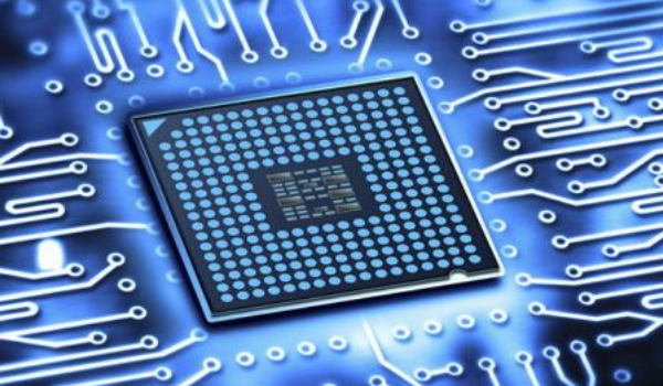
In this comprehensive guide, we will walk through the basic steps and tools needed to delayer, image, and analyze a 7447ic chip to understand how it works. With time, patience, and the right equipment, you can learn to visualize and map out the silicon die, identify components, trace connections, and extract the logic functions to crack any unprotected 7447ic variant.
Necessary Equipment
Cracking an IC requires some specialized equipment to delayer, image, and analyze the chip:
- Delayering tool – A chemical delayering system or micromilling machine to remove packaging and layers from the silicon die.
- Microscope – A microscope with high magnification and camera imaging capabilities for viewing the microscopic IC features.
- Multimeter – A digital multimeter for measuring test points and extracting pinouts.
- Soldering tools – Soldering station, flux, solder, etc. to remove an IC from a PCB.
- Software – Image analysis, diagramming, and data visualization software.
Optional tools like probe stations, logic analyzers, and IC test clips can also help in tracing connections and testing theories. Expect to invest $5,000 to $50,000 for the necessary equipment to get started.
Step 1: Package Removal
The first step is to remove the IC package from the silicon die inside. This is typically a black epoxy case covering the entire chip, with metal leads extending out the sides or bottom.
Use a chemical delayering system to immerse the IC in hot sulfuric acid. This slowly dissolves the epoxy case over several hours until only the bare silicon die remains. Nitric acid can also assist in removing metal lead frames from some package types.
Alternatively, mill away the epoxy case layer by layer using a precision micromilling machine with miniature endmills and diamond cutting tools. This is slower but avoids the hazards of harsh chemicals.
Regardless of the removal method, take care not to damage the delicate silicon die inside when exposing it. Also thoroughly clean and dry the chip before moving to imaging.
Step 2: Die Imaging
With the package removed, the next step is to take high magnification pictures of the die surface. Use a stereo microscope or metallurgical microscope with camera attachment and image stitching software.
Methodically scan the die under magnification in overlapping strips, taking pictures as you move across the surface. Imaging at multiple focal lengths helps capture the full depth of the die. The image stitching software will combine hundreds or thousands of pictures into one giant high-res image file.
Proper lighting is crucial for imaging the microscopic features on an IC. Fiber optic ring lights or controllable surface mounted LEDs positioned at an angle provide the best illumination. 508dpi stadium lights are too big for ICs usually !
Repeat the imaging process after each additional layer is milled away to build up a complete visual map of the full die stack.
Step 3: Layer Delayering
The third step is to sequentially mill or chemically etch away thin layers of the silicon die to reveal the internal features and circuitry layer-by-layer. This process is similar to 3D imaging a CT scan slice by slice.
For micromilling, use progressively finer endmills and lighter passes (5-10um) to slowly grind through the layers. Focused ion beam (FIB) milling is slower but more precise.
Chemical etching with selective etchants can also delineate and exposed the different doped silicon and metal layers. This avoids potential milling damage but requires more care in application.
Repeat the imaging process after removing each layer. Cataloguing and comparing each layer image allows you to build up an understanding of the full 3D IC structure.
Step 4: Component Identification
With die images from the various layers, you can start mapping out the locations of internal logic gates, memory blocks, and other functional components that make up the IC.
Look for clustered arrays and repeating structures like op amps, NAND gates, or shift registers. Identify larger functional blocks like PLLs, ROMs, PWM controllers, etc. Modern ICs often label functional blocks with text markings.
Use visual pattern recognition along with some basic electrical engineering knowledge to deduce the purpose of unfamiliar structures. Having reference images of known logic gates or other components helps with the recognition process when analyzing a new target IC.
Step 5: Connection Tracing
The next major step is tracing how the identified components are interconnected by the metal layers in the die stack. This reverse engineering of the chip’s schematic is the most challenging and tedious part of IC cracking.
Use visual cues, like aligning vias or following metal runs, to incrementally map the circuit paths between components across and between layers. Multi-meter probing and logic analysis on live ICs helps confirm theories on connectivity.
IC camouflaging and other obfuscation techniques intentionally make this tracing step difficult. Be methodical, take notes, and don’t be afraid to start over when hitting a dead end.
Step 6: Logic Extraction
With a complete map of components and connectivity, the final step is analyzing the chip’s functionality to extract the underlying logic operations, algorithms, and programmed data.
Use visual inspection along with logic and math to work out the purpose and interactions of logic sub-circuits. For complex digital ICs, create functional block diagrams and logic flow charts.
In some cases, the IC’s logic can be represented through a system of Boolean algebraic equations, state tables or finite state machine models. Mapping to existing industry standard functions helps identify commonalities.
Thorough documentation is key for replicating or improving upon the target IC’s internal logic in your own designs. This is the culmination of all the previous reverse engineering efforts.
Conclusion
Cracking open and deciphering a 7447ic or other obfuscated IC takes time, care, and perseverance. But the payoff is being able to fully understand and leverage the technology that others try to hide. With this guide, you now have a solid overview of the systematic chip cracking process and skills needed to delayer, image, trace, and analyze ICs.
The world of silicon awaits!
Frequently Asked Questions
Here are some common questions about cracking 7447ic and other ICs:
Q: Is IC cracking legal?
A: Reverse engineering ICs you own is generally legal under fair use exemptions for research and education. However, violating trade secrets or enabling IP theft of chips you don’t own raises legal concerns. Proceed ethically.
Q: Can I crack chips without expensive equipment?
A: Basic delayering and imaging is possible with DIY tools like hot sulfuric acid, sandpaper, and a USB microscope. But commercial-grade tools are highly recommended for professional results.
Q: How long does it take to crack an advanced IC chip?
A: It can take weeks or months of diligent work to completely reverse engineer the most complex ICs with billions of transistors. Simpler chips with only a few layers may only take a couple days.
Q: Do chip makers intentionally make ICs hard to crack?
A: Yes, many techniques like obfuscated wiring, camouflaged gates, and interconnect meshing are used to deter reverse engineering. Cracking gets exponentially harder at smaller process nodes.
Q: What skills does an IC cracker need?
A: Patience, meticulousness, logic/math analysis, basic EE knowledge, photography, and some semiconductor physics. IC cracking requires broad technical skills but rewards persistent effort.