PCB Layout Design Service
Introduction to PCB Layout Design Printed Circuit Board (PCB) layout design is a crucial step in the development of electronic devices. It involves the arrangement of components an
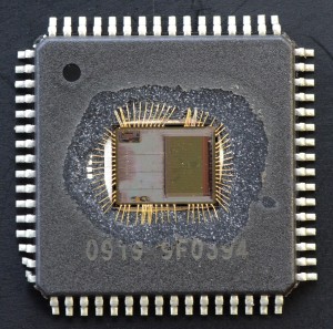
16 years deep in the reverse analysis of integrated circuit technology, senior technical team, skilled, experienced in a variety of blind buried hole PCB , laser blind hole board, UHF board, ceramic board , component density, all over the microstrip lines and other long lines, high-frequency processing requirements and strict control of electromagnetic compatibility of the communication board copy
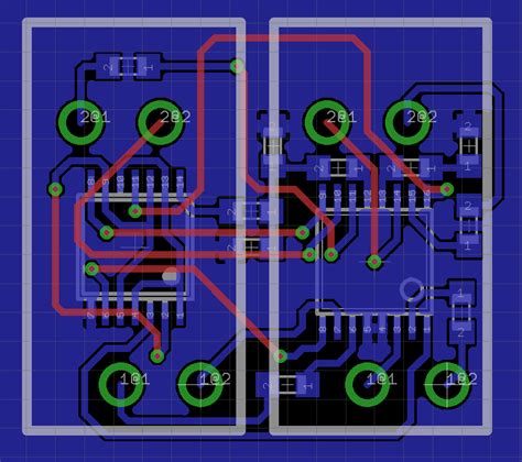
Recent Project
Recent Project
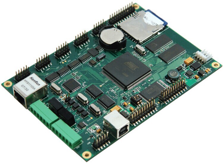
Recent Project
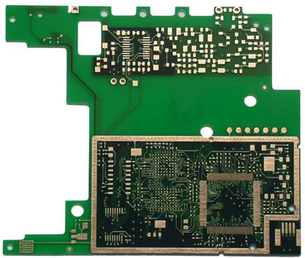
Recent Project
All about PCB Reverse Engineering & IC Crack
Introduction to PCB Layout Design Printed Circuit Board (PCB) layout design is a crucial step in the development of electronic devices. It involves the arrangement of components an
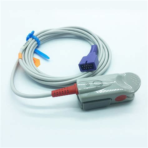
Types of Finger Sensors There are several types of finger sensors, each with its own unique properties and applications. Let's take a closer look at some of the most common types:
What are PCB Slots? PCB slots are elongated openings or cutouts in a printed circuit board that serve specific purposes, such as: Accommodating connectors or other components Prov