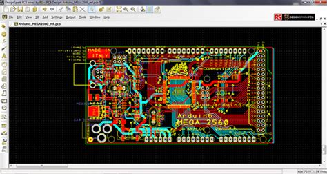
Introduction to DesignSpark PCB
DesignSpark PCB is a powerful, easy-to-use printed circuit board (PCB) design software for Windows PCs. Developed by RS Components, DesignSpark PCB offers a comprehensive set of tools and features for creating professional-grade PCB designs, making it an excellent choice for engineers, hobbyists, and students alike.
Key Features of DesignSpark PCB
- Intuitive user interface
- Extensive component library
- Advanced routing capabilities
- Real-time design rule checking (DRC)
- 3D visualization and export
- Integration with DesignSpark Mechanical
Getting Started with DesignSpark PCB
System Requirements
To run DesignSpark PCB on your Windows PC, ensure that your system meets the following minimum requirements:
| Operating System | Processor | RAM | Free Disk Space | Display Resolution |
|---|---|---|---|---|
| Windows 7/8/10 | 1 GHz | 1 GB | 5 GB | 1024 x 768 |
Installation Process
- Visit the official DesignSpark PCB website (https://www.rs-online.com/designspark/pcb-software) and click on the “Download” button.
- Fill in the required information and agree to the terms and conditions.
- Click on the download link provided in the confirmation email.
- Run the installer and follow the on-screen instructions to complete the installation process.

User Interface Overview
Main Window
The main window of DesignSpark PCB consists of several key areas:
- Menu bar
- Toolbars
- Design area
- Layers panel
- Properties panel
- Library panel
Customizing the Interface
DesignSpark PCB allows you to customize the user interface to suit your preferences:
- Rearrange panels by clicking and dragging them to desired locations.
- Hide or show panels by clicking on their respective icons in the “View” menu.
- Customize toolbar buttons by right-clicking on the toolbar and selecting “Customize.”

Creating a New PCB Project
Project Templates
DesignSpark PCB offers several project templates to help you get started quickly:
| Template | Description |
|---|---|
| Blank | A empty project with default settings |
| Arduino | A project template for designing Arduino Shields |
| Raspberry Pi | A project template for designing Raspberry Pi HATs |
Setting Up Project Properties
Before starting your PCB design, set up the project properties:
- Click on “File” > “Project Options.”
- Configure the following settings:
- Board size and shape
- Number of layers
- Track and via sizes
- Design rules
- Click “OK” to apply the changes.

Designing the Schematic
Adding Components
- Open the Library panel and browse for the required components.
- Drag and drop components onto the schematic canvas.
- Repeat the process until all necessary components are added.
Connecting Components
- Select the “Wire” tool from the toolbar.
- Click on the first component pin to start the connection.
- Click on the second component pin to complete the connection.
- Repeat the process for all required connections.
Assigning Net Names
- Select the “Name Net” tool from the toolbar.
- Click on a wire to assign a name to the connected net.
- Type the desired net name and press Enter.
- Repeat the process for all important nets.
Laying Out the PCB
Placing Components
- Switch to the PCB Layout view by clicking on the “Layout” tab.
- Arrange components on the board by dragging and dropping them into position.
- Consider factors such as component size, orientation, and proximity to related components.
Routing Tracks
- Select the “Route Track” tool from the toolbar.
- Click on the starting pad and then click on the ending pad to create a track.
- Adjust track width and layer as needed.
- Repeat the process for all required connections.
Adding Power and Ground Planes
- Click on the “Planes” icon in the toolbar.
- Select the desired layer and plane type (power or ground).
- Draw the plane outline using the available drawing tools.
- Assign the appropriate net name to the plane.
Design Rule Checking (DRC)
Running a DRC
- Click on “Tools” > “Design Rule Check.”
- Configure the DRC settings based on your PCB manufacturer’s specifications.
- Click “Run DRC” to start the design rule check process.
- Review any reported errors or warnings and make necessary corrections.
Common DRC Errors and Resolutions
| Error | Resolution |
|---|---|
| Clearance violation | Increase the spacing between components or tracks |
| Unconnected net | Ensure all required connections are made |
| Minimum track width | Increase the track width to meet the minimum requirement |
| Hole Size violation | Adjust the hole size to match the specified range |
Generating Manufacturing Files
Gerber Files
- Click on “File” > “Fabrication Outputs” > “Gerbers.”
- Select the layers to include in the Gerber files.
- Configure the output settings, such as file format and aperture list.
- Click “Generate” to create the Gerber files.
Drill Files
- Click on “File” > “Fabrication Outputs” > “NC Drill.”
- Configure the drill file settings, such as units and number format.
- Click “Generate” to create the drill files.
Bill of Materials (BOM)
- Click on “File” > “Assembly Outputs” > “Bill of Materials.”
- Select the desired output format (e.g., CSV, Excel).
- Configure the BOM settings, such as included columns and sorting order.
- Click “Generate” to create the BOM file.
Frequently Asked Questions (FAQ)
1. Is DesignSpark PCB free to use?
Yes, DesignSpark PCB is a free PCB design software provided by RS Components. There are no hidden costs or subscription fees.
2. Can I create multi-layer PCBs with DesignSpark PCB?
Yes, DesignSpark PCB supports the design of multi-layer PCBs. You can specify the number of layers in the project properties.
3. Does DesignSpark PCB have an auto-router?
No, DesignSpark PCB does not include an auto-router. However, it provides powerful manual routing tools and real-time design rule checking to assist in creating optimal PCB layouts.
4. Can I import and export design files from other PCB software?
Yes, DesignSpark PCB supports importing and exporting design files in various formats, such as Eagle, Altium, and KiCad.
5. Is there a community forum for DesignSpark PCB users?
Yes, RS Components hosts an active community forum (https://www.rs-online.com/designspark/forum) where DesignSpark PCB users can ask questions, share knowledge, and collaborate on projects.
Conclusion
DesignSpark PCB is a powerful, user-friendly PCB design software that offers a comprehensive set of features for creating professional-grade PCBs. With its intuitive interface, extensive component library, and advanced routing capabilities, DesignSpark PCB is an excellent choice for engineers, hobbyists, and students looking to design high-quality PCBs on their Windows PCs.