Keywords
- PCB Reproduction
- PCB duplication
- PCB Cloning
- Reverse-Engineering/”>PCB reverse engineering
Understanding the PCB
Before attempting to reproduce a PCB, it is essential to understand its structure and components. A PCB typically consists of the following layers:
- Substrate: The base material, usually made of fiberglass or other insulating materials.
- Copper layers: Thin sheets of copper laminated onto the substrate, forming the conductive pathways.
- Solder mask: A protective layer applied over the copper, leaving only the necessary exposed areas for soldering.
- Silkscreen: A printed layer that adds text, symbols, and logos for easier identification and assembly.
| Layer | Description |
|---|---|
| Substrate | Insulating base material |
| Copper | Conductive pathways |
| Solder Mask | Protective layer over copper |
| Silkscreen | Printed text and symbols |
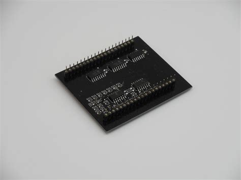
PCB Components
PCBs also contain various electronic components, such as:
- Resistors
- Capacitors
- Inductors
- Diodes
- Transistors
- Integrated Circuits (ICs)
These components are soldered onto the exposed copper areas of the PCB, allowing them to interconnect and form a functional electronic circuit.
PCB Reproduction Methods
There are several methods for reproducing PCBs, each with its own advantages and limitations. The choice of method depends on factors such as the complexity of the board, available resources, and the desired level of accuracy.
1. Manual Tracing
Manual tracing involves carefully examining the original PCB and manually recreating the copper traces and component layouts on a new board. This method is suitable for simple PCBs with few layers and components.
Steps for Manual Tracing
- Clean the original PCB to remove any dirt or debris.
- Use a magnifying glass or microscope to closely inspect the copper traces and component placements.
- Sketch the PCB layout on paper, accurately representing the traces and components.
- Transfer the sketch onto a new PCB substrate using a permanent marker or etch-resistant pen.
- Etch away the unwanted copper areas using a chemical etching solution, leaving only the desired traces.
- Drill holes for through-hole components and vias.
- Apply solder mask and silkscreen layers if necessary.
- Solder the components onto the new PCB.
2. Image-Based Reproduction
Image-based reproduction involves capturing high-resolution images of the original PCB and using image processing software to extract the copper traces and component layouts. This method is more accurate than manual tracing and can handle more complex PCBs.
Steps for Image-Based Reproduction
- Clean the original PCB and ensure it is free from glare and reflections.
- Capture high-resolution images of both sides of the PCB using a digital camera or scanner.
- Use image processing software to enhance the contrast and clarity of the captured images.
- Manually or automatically trace the copper traces and component outlines using the software.
- Convert the traced data into a suitable PCB design format, such as Gerber or ODB++.
- Manufacture the new PCB using the generated design files.
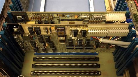
3. X-Ray Imaging
For multi-layer PCBs or boards with hidden traces, X-ray imaging can be used to capture the internal structure of the PCB. This method provides a detailed view of the copper layers and vias, allowing for accurate reproduction.
Steps for X-Ray Imaging
- Place the original PCB in an X-ray machine.
- Capture X-ray images of the PCB from various angles to cover all layers and features.
- Process the captured images using specialized software to extract the layer information and generate a 3D model of the PCB.
- Use the generated 3D model to create the necessary design files for manufacturing the new PCB.
Comparison of Reproduction Methods
| Method | Complexity | Accuracy | Cost |
|---|---|---|---|
| Manual Tracing | Low | Low | Low |
| Image-Based | Medium | Medium | Medium |
| X-Ray Imaging | High | High | High |

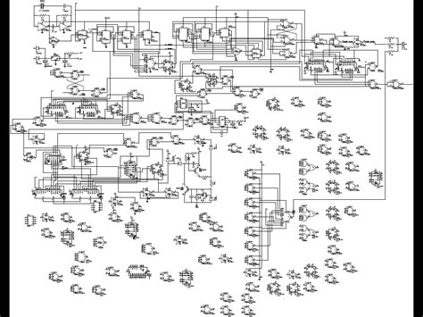
PCB Reverse Engineering
In some cases, reproducing a PCB may require reverse engineering the original design. This involves analyzing the PCB to understand its schematic, components, and functionality. Reverse engineering is particularly useful when the original design files or documentation are not available.
Steps for PCB Reverse Engineering
- Identify the components on the PCB and create a bill of materials (BOM).
- Trace the connections between components and create a schematic diagram.
- Analyze the schematic to understand the circuit’s functionality and identify any sub-circuits or modules.
- Create a new PCB layout based on the reverse-engineered schematic, optimizing the design if necessary.
- Verify the new design by comparing it with the original PCB and conducting functional tests.
PCB Reproduction Services
For those who lack the necessary skills, equipment, or time to reproduce PCBs themselves, there are professional PCB reproduction services available. These services typically offer a range of options, from simple PCB duplication to full reverse engineering and redesign.
Advantages of Using PCB Reproduction Services
- Expertise: Professional services have experienced engineers and technicians who can handle complex PCBs and ensure high-quality results.
- Equipment: Reproduction services have access to advanced equipment, such as X-ray machines and high-resolution scanners, which may not be available to individuals.
- Time-saving: Outsourcing the PCB reproduction process can save significant time and effort, allowing you to focus on other aspects of your project.
Choosing a PCB Reproduction Service
When selecting a PCB reproduction service, consider the following factors:
- Experience: Look for a service with a proven track record of successfully reproducing PCBs similar to yours.
- Capabilities: Ensure that the service has the necessary equipment and expertise to handle your specific PCB reproduction needs.
- Turnaround time: Consider the service’s turnaround time and whether it meets your project deadlines.
- Cost: Compare the costs of different services and choose one that offers the best value for your budget.
Frequently Asked Questions (FAQ)
-
Q: Can any PCB be reproduced?
A: In most cases, yes. However, the complexity of the PCB and the availability of the original design files can affect the feasibility and accuracy of the reproduction process. -
Q: How long does it take to reproduce a PCB?
A: The time required to reproduce a PCB depends on the chosen method and the complexity of the board. Simple PCBs can be reproduced in a matter of hours, while complex boards may take several days or weeks. -
Q: Is it legal to reproduce PCBs?
A: Reproducing PCBs for personal use or repair purposes is generally legal. However, reproducing and selling PCBs without the original designer’s permission may infringe on intellectual property rights. -
Q: What are the costs involved in PCB reproduction?
A: The costs of PCB reproduction vary depending on the method used, the complexity of the board, and the required materials. Professional reproduction services typically charge based on the board’s size, layer count, and the level of reverse engineering required. -
Q: Can I reproduce a PCB with missing components?
A: Yes, it is possible to reproduce a PCB even if some components are missing. However, you will need to identify and source the missing components before assembling the reproduced board.
Conclusion
PCB reproduction is a valuable process for creating identical copies of existing PCBs, whether for replacement, backup, or mass production purposes. By understanding the structure and components of PCBs, and employing the appropriate reproduction methods, you can successfully replicate PCBs with varying levels of complexity. When in doubt, professional PCB reproduction services can provide the expertise and resources necessary to ensure high-quality results.