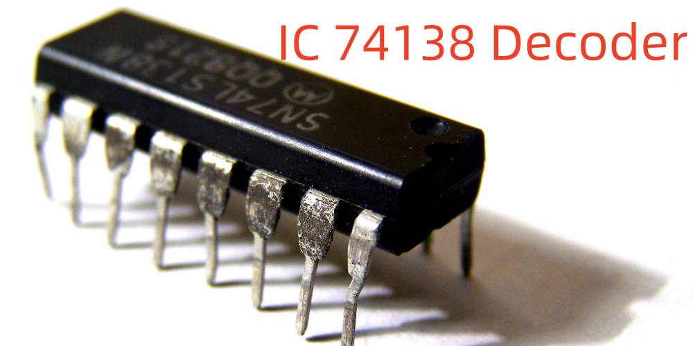
The IC 74138 Decoder works with advanced technology such as the TTL silicon gate technology. They are great for several applications such as decoding a memory address as well as data routing. Usually, these applications come with low utilization of power as well as resistance to loud noises. Present in them are three binary select inputs. Whenever the activation of this IC is done, these pins will decide which of them will become low.
Furthermore, the enable pins come as one high and two lows, which are all active in nature. In addition, the decoder’s output has the ability to drive a ten Schottky equal load of low power. All inputs will then be protected from any harm because of the static discharge that happens with diodes and towards the ground and the VCC.
In this article, we will be discussing the applications and all you need to know about the IC 74138 Decoder.
What is the IC 74138 Decoder?
The IC 74138 Decoder can be described as a IC decoder of three to eight lines. Its main function is decoding multiple applications. This IC’s setup is accessible only with a setup between three inputs and eight outputs. In addition, the IC serves in applications such as memory decoding as well as routing of data. In addition, you can use these ICs for reducing the decoding effects of the systems in the high performance memory systems.
Also, the IC 74138 decoder features three different enable pins. Two of these pins are usually less active, while the third one is usually very active. All three pins help in decreasing the significance and need for using the outside gates. You can implement the 24 line decoders without having to make use of the outer inverters coupled with the 32 line decoders that require one inverter.
Furthermore, this IC 74138 decoder is mainly utilized for different de-multiplexing applications using enable pins such as data input pins. Also, this IC’s inputs are usually clamped with the Schottky diodes. These work with high performance and they help in containing line ringing coupled with simplifying the design of a system.
What are the Features of the IC 74138 Decoder?
First, the IC 74138 Decoder is specifically designed for high-speed applications. Also, it has a great decoding capacity and it ensures the security of the ESD.
Furthermore, it ensures unbiased delays in propagation and incorporates the three enable pins to ensure that cascading is simplified. In addition, its supply Voltage usually ranges between 1.0V and 5.5V. The inputs usually permit voltages that are superior to the VCC. Its Standard delay in propagation is usually 21ns.
Another great feature of the IC 74138 Decoder is its low consumption of power at just -32mW. To ensure it delivers high performance, this decoder is usually Schottky clamped.
Lastly, to operate the IC 74138 Decoder, you will need a temperature that falls within -40 degrees Celsius and 125 degrees Celsius.
What are the Applications of the IC 74138 Decoder?
IC decoders are mainly manufactured to work effectively in memory decoding as well as applications relating to data routing.
This application’s performance is dependent on the rate of data exchange, and this is why there must not be any delay. In addition, this IC 74138 decoder works effectively in several applications. This is because they have lower delay times compared to the memory’s access time. Therefore, we can say that this effective system will not impact its performance.
In addition to routing of data, the IC 74138 decoder works effectively for several applications. There are applications that need high noise resistance and low consumption of power. Also, the main feature of this decoder is decoding of digital signals. Other applications can be found in the demultiplexing of the digital signals as well as the digital memory circuit. Other applications of the IC 74138 decoder are found in servers, telecom circuits, line decoders, memory circuits, as well as digital systems.
Understanding the IC 74138 Decoder Pins
There are sixteen pins here. Let’s consider them.
For power inputs, Vcc and ground pins are available. There are three input pins present. They are described as A0, A1, and A2. This is why this decoder has the ability to accept three binary input signals
It also features three input pins. They are described as E1, E2, and E3. The first two are described as the active and LOW pins. When low signals are applied onto them, they become extremely active. Furthermore, eight output pins are available
Using the IC 74138 Decoder
In order to have a good understanding of the way the IC 74138 Decoder works, we need to design a circuit that has the necessary electronic components.
Here, these outputs lean towards the LED (Light emitting diodes) so as to describe which of the o/p pins will go low and which of the IC outputs would be inverted.
We will make use of just one device to ensure that the connections of both the G2B pins and G2A pins are well connected to the GND. This is then followed by a linkage between the G1 pins and the VCC to help in chip activation.
Furthermore, for the device, three buttons help in signifying three i/p lines. Also, note that immediately the connection of the enable pins has been done, then you can connect the input to get the output.
Conclusion
We hope this post has explained what the IC 74138 Decoder is. In summary, the IC 74138 Decoder can be described as an IC decoder of three to eight lines. Its main function is decoding multiple applications. This IC’s setup is accessible only with a setup between three inputs and eight outputs. In addition, the IC serves in applications such as memory decoding as well as routing of data. Also, you can use these ICs for reducing the decoding effects of the systems in the high performance memory systems. The IC 74138 Decoder works with advanced technology such as the TTL silicon gate technology.