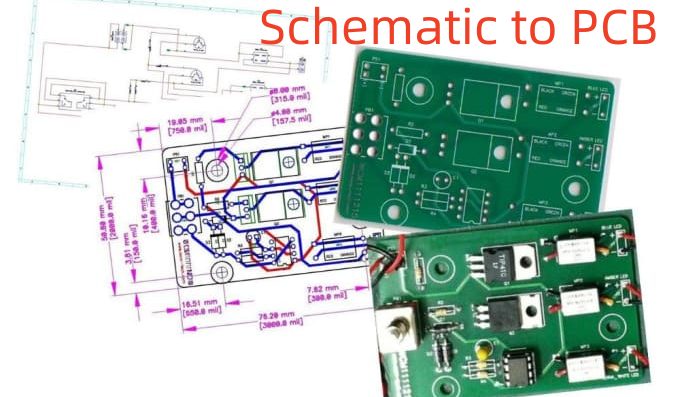
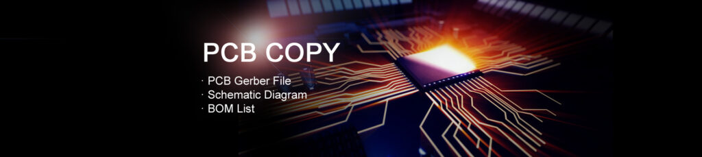
If you belong to the PCB field, then you might have often heard of this technique. PCB reverse engineering is simply PCB copying. We can easily develop replicas of PCBs through this technique.
It comes in handy when we are talking about large-scale production of PCBs in less time. When we use this method, we can analyze all the components of pre-existing PCBs to develop their copies.
The reports on PCB reverse engineering, therefore, help us with the details as well. Experts believe that PCB reverse engineering is less complex because it promises great results, plus it never compromises the PCB components that are sensitive and critical. You also need to keep in mind that PCB reverse engineering needs highly trained technicians to perform the method professionally.
Other than this, the process will become complicated, and its challenges can become irreversible later.
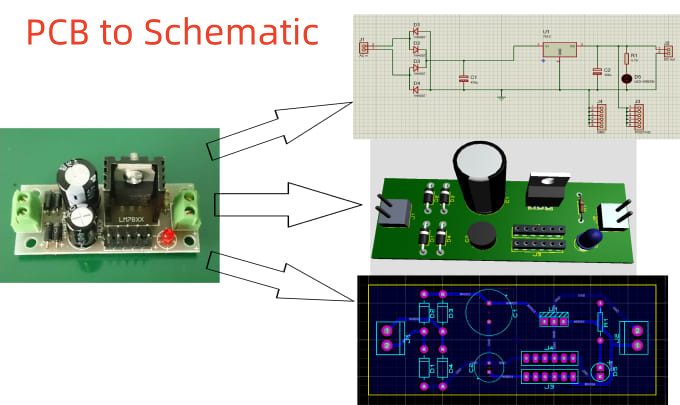
How Reverse Engineering PCB To Schematic Work?
If you have been wondering if this method can help us with reverse engineering and PCB design development, then think no further. It is absolutely possible.
The reason is that through PCB reverse engineering, we can take help from several other techniques to gain good results. Reverse engineering is also important to consider to develop complex designs in just less time, unlike former PCB development, which could extend up to several years.
Since technology has made producers use different methods to speed up their operations, there is no doubt that PCB reverse engineering is one of them. We can get done with the critical PCB designing steps easily with reverse engineering.
The Procedure Of Reverse Engineering PCB To Schematic
Reverse engineering is important in the field of PCB. However, we need to make sure to execute it in a proper way to get the desired results. Therefore, we have divided this process into a few steps for the sake of your ease. Take a look:
- Draw the circuits, do scanning, and capture the circuits.
- Edit and upload the images and photographs to the software.
- Copy the pre-existing design by going from layer to layer.
- Developing circuit schematics at the end.
In general, PCB reverse engineering comprises these four crucial steps. Consider them as your checklist while you are performing reverse engineering so that you can make sure to complete all the essential steps of this process easily.
Procedure Of Reverse Engineering PCB To Schematic – A Single-Sided Board
Yes, we can perform reverse engineering on a single-sided board. However, there are some tips for it that you need to keep in mind. First off, start by visualizing and identifying the PCB components and determine your budget. Make sure to procure quality production materials that come under your budget.
After this, make sure to click photographs of the PCB that you want to reverse engineer. The next step is to separate the PCB components and then compare them with the photographs by mapping them out on the pictures. Also, scanning the PCB itself is crucial because it will give you a vivid idea about the production of a new clone of PCB. Now you can start mounting PCB components on the clone.
Reverse Engineering PCB To Schematic – A Double-Sided Board
When it comes to PCB reverse engineering for dual-sided boards, then there are some things that you need to take care of. It is because double-sided boards are complex and need your undivided attention. First off, make sure to mention the type and model of PCB for reverse engineering. Adjust the components as well. Make sure that you are carefully positioning the components like transistors, resistors, and capacitors. Negligence in their positioning can alter the results in the end. Now it leads us to the desoldering of components on pre-existing PCB. You also need to carefully detach the pads from their corresponding vias. There should not be any lettering because it leads to the formation of silkscreen. You can even rub and polish the layers to get precise results. It will enhance the shine of copper traces as well.
Other than this, it is important to set the contrast of the canvas. You have to be careful with the background so that you can get HD pictures of PCBs. It is an important point. It is because, without a proper collection of PCB photographs from different angles, you cannot expect great results from PCB reverse engineering. Keep in mind that you cannot rush with the PCB reverse engineering.
It is because every step requires precision, and the margin of error is also really less. Once you are done with reverse engineering, you can easily do the final checking. Since it will help you identify the faults and with last-minute changes, you can ensure 100% quality of your PCB clones for your clients.
Reverse Engineering PCB To Schematic – A Multi-Layered Board
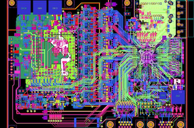
The PCB reverse engineering process for the multi-layered boards is not different from the abovementioned ones. The reason is that you need to prepare all the details for the process. Plus, it also includes capturing your PBCs and uploading the images to the software. You also need to carefully place the PCB components to avoid complications.
When we talk about multi-layered PCBs, we need to separate the high components, and only the SMD components remain on the PCB. Also, experts believe that you should not misplace the photographs at this point of the process because photographs are a great way to perform the process with the least hustle. Plus, you can easily get an idea about the properties and structure of PCBs through these pictures. Determining your budget is also crucial. You need to get your hands on quality materials with the least investment.
For the desoldering purpose, a hot air gun is beneficial. Billing is important for each PCB component because it not only helps in procuring exceptional and industrial-grade materials for production but also helps in effortless arrangements and supply. Now you know that you can easily perform PCB reverse engineering on different types of PCBs to develop their clones. Well, PCB reverse engineering has a lot of aspects. Therefore, we cannot describe all of them at once since it will become overwhelming for you. In the next section, we are going to take a brief look at the pros and cons of PCB reverse engineering.
Pros And Cons Of Reverse Engineering PCB To Schematic
PCB reverse engineering is the lifeblood of the PCB field. However, just like everything has its downsides, PCB reverse engineering has its own.
Therefore, in this section, we will shed light on the pros and cons of PCB reverse engineering for you so that you can easily decide whether this method is for you or not. There is no doubt that you ensure 100% quality with the method. From pre-existing PCBs to newly developed PCB replicas, everything showcases precision and quality. The methods like PCB reverse engineering allow us to use these PCB replicas in technical fields like automotive and aerospace. In case of defects and faults, we can use reverse engineering, which is an affordable method to perform for this purpose. But if we look at the other side of the image, we will come to know that PCB reverse engineering is not suitable for several fields, and defense is one of them.
Other than this, the nature of PCB reverse engineering is also complex. Therefore highly skilled technicians are required to perform the method to avoid complications. Due to this reason, some producers find it hard in terms of talent acquisition to perform PCB reverse engineering effortlessly without any complications.
Sometimes the problems that occur in PCB reverse engineering can get out of hand. Due to this reason, special equipment and rare materials are needed to counter these problems. This, again, disturbs the budget of producers and makes the process expensive for them. Now you have a clear idea about the pros and cons of PCB reverse engineering. You can now decide whether you can afford to perform this method in your operations or not.
Why PCB Reverse Engineering Is Standard?
You might have thought about it as well. You need to know that why PCB reverse engineering has been successful in gaining a soft spot in the lives of PCB producers. Today, about 60%-70% of PCB producers rely on PCB reverse engineering to gain great results. Let’s check these reasons below:
- Ensuring more quality for the PCBs and their components is the ultimate goal of the day for PCB producers. Reverse engineering makes it possible and sheds a burden on the shoulders of the producers to a large extent.
- Reverse engineering settles with a producer’s budget easily. It means it saves you from investing in redundant steps, materials, and production equipment on all counts.
- With reverse engineering, you are making PCB parts more efficient. This comes in handy in the complex applications and devices that fully depend on such PCBs for extensive functioning.
- The replacement also becomes easier, and the process becomes affordable for the producers due to PCB reverse engineering.
Conclusion
PCB reverse engineering has been there in the field for many years. It has led to the development of industrial-grade PCB clones. Clients and producers both have been satisfied with its results. If you are a producer who lacks knowledge about PCB reverse engineering, then it is better to take help from this post and research further. Other than this, we have also discussed the pros and cons of PCB reverse engineering so that you can make an effective decision for yourself.