The PCB Assembly Process: An Overview
Before diving into the tips, let’s review the main steps of the PCB assembly process at a high level:
-
Design & Manufacturing: It all starts with the PCB design, which is created using EDA (electronic design automation) software. The design is used to manufacture the bare PCB.
-
Solder Paste Application: Solder paste, a mixture of tiny solder balls and flux, is precisely applied onto the PCB pads using a stencil.
-
Component Placement: The electronic components are placed onto their respective positions on the PCB, on top of the solder paste. This is typically done by a pick-and-place machine.
-
Reflow Soldering: The populated PCB goes through a reflow oven, which melts the solder balls in the paste, permanently attaching the components to the PCB pads.
-
Inspection & Testing: The assembled PCB undergoes various inspections (visual, x-ray, electrical testing, etc.) to verify proper assembly and functionality before moving on to subsequent processes.
Now that we’ve outlined the key steps, let’s explore the 9 tips to optimize your PCB assembly process.
Tip 1: Design for Manufacturability (DFM)
One of the most important things you can do to ensure smooth PCB assembly actually happens before the assembly process even begins – during the PCB design phase. Designing with manufacturability in mind from the start can prevent many potential issues down the line.
Some key DFM considerations include:
- Choosing appropriate component packages and sizes
- Providing adequate spacing between components
- Using standard drill hole and trace sizes
- Specifying proper solder mask and silkscreen
- Adding fiducials for machine vision alignment
By optimizing your design for assembly, you can avoid problems like tombstoning of small components, solder bridges, insufficient clearances for assembly machines, and more. Always involve your PCB manufacturer early in the design process to get their DFM feedback.

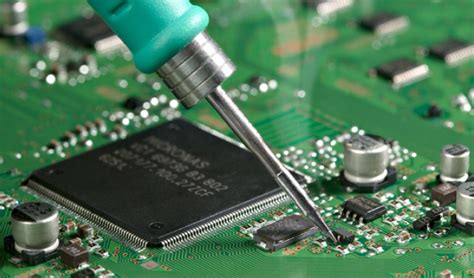
Tip 2: Use Solder Paste Stencils
Solder paste is the “glue” that holds components onto the PCB pads during reflow. Consistent solder paste application is critical for good solder joints. While you can apply paste by hand for prototypes or small batches, solder paste stencils are a must for larger production.
A stencil is a thin sheet of stainless steel with laser-cut openings matching your PCB’s solder pad pattern. It’s placed over the PCB and solder paste is spread across it with a squeegee blade, depositing paste only on the exposed pads.
Using a stencil provides several advantages:
- Precise control over paste volume and position
- Even distribution of paste
- Minimizes bridging and other soldering defects
- Faster and less messy than applying paste by hand
Make sure to choose the right stencil thickness for your paste and PCB. Common stencil thicknesses range from 0.004″ to 0.008″. Thinner stencils are used for finer pitch components. Your stencil supplier can recommend the optimal thickness based on your PCB design.

Tip 3: Maintain Proper Reflow Profile
Reflow soldering involves heating the PCB assembly in an oven to melt the solder paste, forming permanent solder joints. The temperature profile the PCB experiences over time in the oven is called the reflow profile.
Maintaining the right reflow profile is key to forming reliable solder joints while preventing component and PCB damage from excess heat. The ideal profile depends on your solder paste, PCB thickness, and component mix.
A typical reflow profile looks like this:
| Stage | Temperature | Duration |
|---|---|---|
| Preheat | 150-200°C | 60-120 sec |
| Soak | 150-200°C | 60-120 sec |
| Reflow | 220-250°C | 30-90 sec |
| Cooling | < 100°C | 30-90 sec |
The key steps are:
- Preheat – Gradually ramps up the temperature to activate the flux and dry the paste.
- Soak – Holds temperature to allow an even distribution of heat across the assembly.
- Reflow – Quick spike above the solder melting point to form the solder joints.
- Cooling – Gradual cool down to solidify joints and prevent thermal shock.
Most reflow ovens have built-in profiling capabilities to monitor and control the exact temperatures over time. For consistent results, regularly verify and calibrate your oven’s profile.

Tip 4: Keep PCB & Components Moisture-Free
Moisture is one of the biggest enemies of PCB assembly. If PCBs or components absorb too much moisture from humidity in the air, that moisture can turn into steam and cause defects during reflow.
Some common moisture-related defects include:
- Popcorning – Cracking or “popping” of plastic component packages
- Delamination – Separation of PCB layers due to vapors
- Spattering – Small balls of solder splattered due to explosive moisture evaporation
- Solder voids – Gaps in solder joints where steam pushed out the molten solder
To prevent moisture issues:
- Bake PCBs and moisture-sensitive components before assembly to drive off absorbed moisture
- Store PCBs and components in moisture-barrier bags with desiccant
- Assemble boards soon after opening moisture-sealed packages
- Control humidity in the assembly area
Refer to the IPC/JEDEC J-STD-020 standard which classifies moisture sensitivity levels (MSLs) for components and provides handling guidelines to avoid moisture damage.
Tip 5: Use SPI & AOI Systems for Inspection
Manually inspecting every PCB assembly under a microscope is time-consuming and error-prone. Fortunately, automated optical inspection (AOI) and solder paste inspection (SPI) systems make inspection faster and more reliable.
SPI systems inspect the solder paste deposit after stencil printing. They use 2D or 3D machine vision to verify:
- Paste presence and position on every pad
- Paste height, area, and volume
- Bridging or other solder paste defects
Catching paste issues early allows correcting stencil alignment or paste consistency before components are placed, saving time and materials.
After reflow, AOI systems verify the assembled PCB by checking:
- Presence, position, and polarity of components
- Solder joint shapes and fillets
- Bridging, tombstoning, and other solder defects
While AOI doesn’t catch every defect, it rapidly screens for common issues and greatly reduces dependency on human inspection. SPI and AOI are well worth the investment for any volume PCB assembler.
Tip 6: Clean Flux Residues
After reflow soldering, there is usually some flux residue remaining on the PCB from the solder paste. While some fluxes are “no-clean” and don’t require removal, others must be cleaned to prevent issues like:
- Corrosion from active flux ingredients
- Dendritic growth leading to short circuits
- Interference with electrical testing probes
- Poor adhesion of conformal coatings
Flux residues are typically cleaned by washing the PCB with solvents or water-based detergents formulated for electronic cleaning. Common cleaning methods include:
- Batch immersion in an ultrasonic cleaner tank
- Inline conveyorized spray washing
- Manual spraying or brushing for rework
If using a no-clean flux, verify it’s truly benign for your application before skipping cleaning. Always clean any visible flux residues, even with no-clean fluxes.
Tip 7: Implement ESD Controls
Static electricity is a significant threat to the electronically sensitive components on a PCB. Electrostatic discharge (ESD) occurs when a statically-charged object touches an electronically-conducting object, releasing a high voltage spark.
ESD can cause PCB component failures from:
- Catastrophic destruction from arcing
- Latent defects that escape testing but fail prematurely
- Incremental weakness from cumulative ESD exposure
To protect PCBs from ESD damage during assembly, follow these controls:
- Ground all conductive work surfaces, tools, and machinery
- Connect workers to ground with wrist straps or ESD footwear
- Use static dissipative mats and flooring
- Ionize the air to neutralize static charges
- Handle boards and components in static-shielding bags
Train all personnel in ESD awareness and prevention. Regularly audit your ESD controls using static field meters and other test equipment. Refer to the ANSI/ESD S20.20 standard for a complete guide to ESD control in electronics manufacturing.
Tip 8: Manage Component Inventory
Keeping track of your electronic component inventory is essential for an efficient PCB assembly process. Running out of a component mid-production can cause expensive delays.
Some tips for effective component inventory management:
- Use a computerized MRP/ERP system to track stock levels and forecast requirements
- Set reorder points and safety stock buffers for each part
- Regularly cycle count inventory and reconcile discrepancies
- Avoid excess inventory that ties up cash and may become obsolete
- Label parts clearly with part numbers, quantities, and date codes
- Use first-in-first-out (FIFO) picking to avoid expired parts
- Securely store moisture-sensitive parts in dry cabinets or nitrogen storage
In addition to quantity, also manage component quality. Verify the authenticity of components to avoid counterfeits. Inspect parts for bent pins, damage, or signs of prior use. Segregate non-conforming parts to prevent mixing with good inventory.
Tip 9: Document & Continuously Improve the Process
Finally, no PCB assembly process is static. To maintain and improve your process over time, it’s essential to document it and continuously make improvements.
Create clear work instructions, machine settings recipes, inspection checklists, and other documentation to standardize your process. Use photos and videos to provide clarity. Make documents easily accessible to operators on the production floor.
Establish metrics to measure the performance of your process, such as:
- First pass yield
- Defects per million opportunities (DPMO)
- Cycle time per assembly
- On-time delivery to customers
Review metrics regularly and conduct root cause analysis on any issues or defects that arise. Implement corrective actions and preventive actions (CAPAs) to address problems at the source.
Engage your operators in continuous improvement activities like Kaizen events or suggestion systems. Encourage them to propose process enhancements and solve problems.
Audit your process periodically using tools like layered process audits (LPAs). Compare your procedures against IPC standards and best practices. Identify and close any gaps.
By methodically documenting, measuring, and improving your PCB assembly process, you can achieve world-class quality, productivity, and customer satisfaction.
Frequently Asked Questions
Q1: What is the difference between wave soldering and reflow soldering?
A1: Wave soldering and reflow soldering are two different methods of soldering components to a PCB:
- Wave soldering involves passing the PCB over a molten wave of solder. It’s typically used for through-hole components on the bottom side of the board.
- Reflow soldering uses solder paste applied to the PCB pads. Components are placed on top of the paste, then the entire assembly is heated in an oven to melt and reflow the solder. It’s used for surface mount components.
Q2: What is the purpose of PCB Conformal Coating?
A2: Conformal coating is a thin polymeric film applied onto a PCB assembly to protect it from environmental hazards. It offers benefits like:
- Moisture and corrosion resistance
- Electrical insulation
- Protection from tin whiskers
- Mechanical support for components
Common conformal coating materials include acrylic, silicone, urethane, and parylene. Coating is typically applied by spraying, brushing, or dipping after the PCB is fully assembled.
Q3: How do I select the right solder paste?
A3: Selecting the right solder paste involves considering several factors:
- Alloy composition – Match the paste alloy to the environmental requirements and component metallizations. Common alloys are tin-lead, SAC305, and SN100C.
- Powder particle size – Choose powder size based on the smallest stencil aperture or narrowest pitch. Sizes range from Type 2 to Type 6, with Type 4 being most common.
- Flux activity – Select flux activity (low, medium, high) based on the oxidation of the surfaces to be soldered. Higher activity for more oxidized surfaces.
- Viscosity – Choose viscosity based on print speed, aperture size, and board topology. Higher viscosity for finer pitches and larger apertures.
Consult with your solder paste supplier for recommendations based on your specific application.
Q4: What are some common PCB assembly defects?
A4: Some of the most common defects encountered in PCB assembly include:
- Bridging – Solder shorts between adjacent pads or pins
- Tombstoning – One end of a chip component lifting off the pad
- Poor wetting – Incomplete solder coverage or adhesion to a surface
- Solder balls – Small spheres of solder stuck to the PCB or components
- Insufficient or excess solder – Too little or too much solder on a joint
- Component shift – Movement of components during reflow
- Lifted pads – Pads separated from the PCB due to mechanical stress
Many of these defects can be prevented by following DFM guidelines, using SPI/AOI, and maintaining a well-controlled assembly process.
Q5: How do I choose a PCB assembly partner?
A5: If you’re outsourcing your PCB assembly, selecting the right contract manufacturer (CM) is critical. Look for a CM with:
- Experience in your industry and product type
- Capability to handle your volumes and technology needs
- Quality certifications like ISO 9001, ISO 13485, or AS9100
- Automated assembly and inspection equipment
- Robust quality and process control systems
- Flexibility to scale up and support your growth
- Good communication and customer service
- Competitive pricing and lead times
Request references, audit their facility, and start with a small trial order before committing to a high-volume production run. Building a close partnership with your CM can make a huge difference in your product’s success.
Conclusion
PCB assembly is a complex process with many variables that can impact the quality and reliability of the final product. By understanding the key steps involved and following the 9 tips outlined in this guide, you can ensure a smoother, more efficient assembly process.
Remember to design for manufacturability, use solder paste stencils, maintain proper reflow profiles, keep moisture under control, leverage automated inspection, clean flux residues, implement ESD controls, manage component inventory, and continuously document and improve your process.
Whether you’re assembling PCBs in-house or outsourcing to a contract manufacturer, investing time and resources into optimizing your PCB assembly process will pay off in higher yields, fewer defects, and happier customers in the long run.