What is a PCB Prototype?
A PCB (Printed Circuit Board) prototype is a preliminary version of a printed circuit board that is used for testing and validation before mass production. It is an essential step in the electronics design process, allowing engineers and designers to verify the functionality, performance, and reliability of their PCB design.
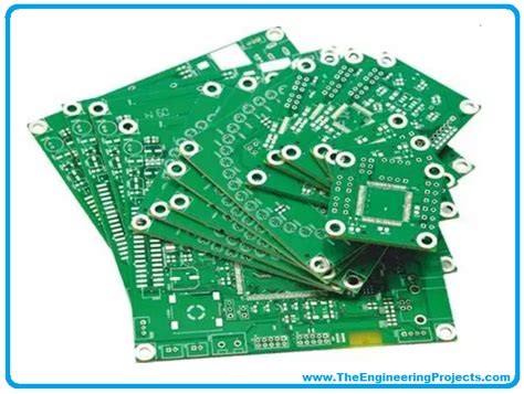
PCB prototypes are typically manufactured in small quantities, ranging from a single unit to a few dozen boards. They are created using the same materials and processes as the final production PCB but may have some differences in terms of component placement, routing, or overall layout.
Types of PCB Prototypes
There are several types of PCB prototypes, each serving a specific purpose in the design process:
-
Visual Prototype: A non-functional PCB that represents the physical layout and dimensions of the final board. It is used for visual inspection and to ensure proper fit in the intended enclosure.
-
Proof-of-Concept (POC) Prototype: A functional PCB that demonstrates the basic functionality of the design. It may not include all the features or components of the final product but serves to validate the core concept.
-
Functional Prototype: A fully functional PCB that includes all the components and features of the final product. It is used for extensive testing, debugging, and performance optimization.
-
Pre-Production Prototype: A PCB that is manufactured using the same processes and materials as the final production board. It is used for final testing and certification before mass production begins.
Why You Need a PCB Prototype
1. Design Validation
One of the primary reasons for creating a PCB prototype is to validate the design before committing to mass production. By testing a physical prototype, engineers can identify and correct any design flaws, such as incorrect component placement, signal integrity issues, or power distribution problems.
Catching these issues early in the design process can save significant time and money, as making changes to a PCB design becomes increasingly expensive as the project progresses.
2. Functionality Testing
A functional PCB prototype allows engineers to test the board’s performance under real-world conditions. This includes verifying the functionality of individual components, ensuring proper communication between different parts of the circuit, and measuring key parameters such as power consumption, signal quality, and electromagnetic compatibility (EMC).
By thoroughly testing the prototype, engineers can optimize the design for better performance, reliability, and efficiency.
3. Manufacturability Assessment
Creating a PCB prototype also helps assess the manufacturability of the design. This involves evaluating factors such as component placement, routing density, and overall board complexity to ensure that the PCB can be efficiently and reliably manufactured in large quantities.
By working with a PCB manufacturer during the prototyping phase, designers can receive valuable feedback on how to optimize their design for mass production, reducing the risk of manufacturing issues down the line.
4. Compliance Testing
Many electronic products must comply with various industry standards and regulations, such as FCC (Federal Communications Commission) rules for electromagnetic interference (EMI) or UL (Underwriters Laboratories) safety standards.
A PCB prototype can be used to conduct compliance testing, ensuring that the design meets all the necessary requirements before proceeding with mass production. This helps avoid costly redesigns or certification delays later in the development process.
5. Demonstration and Fundraising
For startups and entrepreneurs, having a functional PCB prototype can be a valuable tool for demonstrating their product to potential investors or customers. A working prototype provides tangible evidence of the product’s feasibility and can help secure funding or generate interest from early adopters.

The PCB Prototyping Process
The PCB prototyping process typically involves the following steps:
-
Schematic Design: The first step is to create a schematic diagram of the circuit, which represents the electrical connections and components in the system.
-
PCB Layout: Using the schematic as a guide, the PCB layout is designed using specialized software. This involves placing components and routing traces on the board to create the desired electrical connections.
-
Design Review: The PCB layout is reviewed for errors, manufacturability, and compliance with design rules and industry standards. Any necessary revisions are made at this stage.
-
Prototype Fabrication: The PCB design files are sent to a PCB manufacturer for prototype fabrication. This typically involves the following sub-steps:
- Printing the circuit pattern onto a copper-clad board using photolithography
- Etching away the unwanted copper to create the desired traces
- Drilling holes for through-hole components and vias
- Applying solder mask and silkscreen layers
-
Cutting the board to its final shape
-
Component Assembly: Once the bare PCB is fabricated, the components are soldered onto the board, either manually or using automated assembly processes.
-
Testing and Debugging: The assembled PCB prototype is tested for functionality and performance, and any issues are debugged and corrected.
-
Design Iteration: Based on the testing results and feedback, the PCB design may undergo further iterations to optimize performance, reliability, or manufacturability.

Choosing a PCB Prototyping Service
When selecting a PCB prototyping service, consider the following factors:
-
Capabilities: Ensure that the service can accommodate your specific requirements, such as board size, layer count, material selection, and component density.
-
Turnaround Time: Consider how quickly you need your prototypes and choose a service that can meet your timeline.
-
Quality: Look for a service with a proven track record of producing high-quality PCBs, with strict quality control processes in place.
-
Cost: Compare pricing from multiple services, but be cautious of sacrificing quality for lower costs.
-
Support: Choose a service that offers good customer support and can provide guidance throughout the prototyping process.
| Service | Capabilities | Turnaround Time | Quality | Cost | Support |
|---|---|---|---|---|---|
| PCBWay | High | Fast | High | Moderate | Excellent |
| JLCPCB | High | Fast | High | Low | Good |
| OSH Park | Moderate | Moderate | High | Moderate | Good |

Frequently Asked Questions (FAQ)
1. How long does it take to get a PCB prototype?
The turnaround time for PCB prototypes varies depending on the complexity of the design and the chosen prototyping service. Some services offer quick turnaround times of 24-48 hours for simple designs, while more complex boards may take several days or weeks.
2. How much does a PCB prototype cost?
The cost of a PCB prototype depends on factors such as the board size, layer count, material selection, and quantity. Simple, low-quantity prototypes can cost as little as a few dollars per board, while more complex designs or higher quantities can cost hundreds or even thousands of dollars.
3. What files do I need to provide for PCB prototyping?
To have your PCB prototype manufactured, you typically need to provide the following files:
- Gerber files: These are the industry-standard files that describe the PCB layout, including the copper layers, solder mask, and silkscreen.
- Drill files: These specify the location and size of holes in the PCB.
- Bill of Materials (BOM): A list of all the components used in the design, including their reference designators, values, and package types.
- Assembly drawings: Diagrams that show the placement of components on the PCB.
4. Can I assemble my own PCB prototype?
Yes, it is possible to assemble your own PCB prototype, especially for simpler designs. However, this requires access to the necessary tools and equipment, such as a soldering iron, reflow oven, and surface mount technology (SMT) placement machine. For more complex designs or higher quantities, it is often more practical and cost-effective to use a professional assembly service.
5. What should I do if my PCB prototype doesn’t work as expected?
If your PCB prototype does not function as intended, follow these steps:
- Visually inspect the board for any obvious manufacturing defects or assembly issues.
- Double-check the component placement and orientation against the assembly drawings.
- Use a multimeter or oscilloscope to test for continuity and proper voltage levels.
- Review the schematic and PCB layout for any design errors.
- Consult with the prototyping service or a professional PCB designer for further guidance and support.
Conclusion
PCB prototyping is a crucial step in the electronics design process, allowing engineers and designers to validate their designs, test functionality, assess manufacturability, and ensure compliance with industry standards. By carefully selecting a prototyping service and following best practices for design and testing, you can create high-quality PCB prototypes that pave the way for successful mass production.
Remember, investing time and resources into thorough prototyping can save significant costs and headaches down the line, ultimately leading to a better end product. So, don’t skimp on this essential step in your electronics design journey.