The Importance of PCB Design
PCB design plays a critical role in the performance, reliability, and manufacturability of electronic products. A well-designed PCB ensures that:
- Signals are routed correctly between components
- Power and ground are distributed effectively
- Electromagnetic interference (EMI) is minimized
- Thermal management is optimized
- The board is manufacturable at scale
Poor PCB design can lead to a host of issues, such as signal integrity problems, power distribution failures, excessive EMI emissions, thermal hotspots, and manufacturing defects. These problems can result in product malfunctions, reduced reliability, increased costs, and delayed time-to-market.
The PCB Design Process
The PCB design process typically involves several key steps:
-
Schematic capture: The first step is to create a schematic diagram that shows how all the components are connected electrically. This is done using electronic design automation (EDA) software.
-
Component placement: Once the schematic is complete, the next step is to place the components on the board layout. The placement is optimized for signal routing, power distribution, thermal management, and manufacturability.
-
Routing: After the components are placed, the copper traces are routed to interconnect them according to the schematic. The routing is done in accordance with design rules that specify parameters such as minimum trace width, clearance between traces, via sizes, etc.
-
Design rule check (DRC): A DRC is performed to verify that the board layout complies with all the design rules. Any violations are flagged and corrected.
-
Output generation: Finally, the PCB design software generates the output files needed for manufacturing, such as Gerber files, drill files, and bill of materials (BOM).
Here is a table summarizing the key steps in the PCB design process:
| Step | Description |
|---|---|
| Schematic capture | Create a schematic diagram showing component connections |
| Component placement | Place components on the board layout optimized for various factors |
| Routing | Route copper traces to interconnect components per the schematic |
| Design rule check | Verify the board layout complies with all design rules |
| Output generation | Generate the files needed for PCB manufacturing |
PCB Design Considerations
There are many factors that need to be considered during PCB design to ensure optimal performance, reliability, and manufacturability. Some of the key considerations include:
Signal Integrity
Signal integrity refers to the quality of the electrical signals transmitted through the PCB. Factors that can affect signal integrity include:
- Trace impedance: The impedance of the traces needs to be controlled to match the impedance of the source and load to minimize reflections.
- Crosstalk: Crosstalk occurs when signals on adjacent traces interfere with each other. It can be minimized by proper trace spacing and the use of guard traces.
- Transmission line effects: At high frequencies, traces behave like transmission lines and need to be terminated properly to prevent reflections.
Power Integrity
Power integrity refers to the quality of the power distribution network on the PCB. Factors that can affect power integrity include:
- Voltage drop: The resistance of the power traces can cause a voltage drop that affects the performance of the components.
- Decoupling: Decoupling capacitors are used to provide a local source of charge to the components and reduce noise on the power supply.
- Power plane resonance: The power and ground planes can resonate at certain frequencies, causing noise and signal integrity issues.
Electromagnetic Compatibility
Electromagnetic compatibility (EMC) refers to the ability of the PCB to function properly in its electromagnetic environment without causing or suffering from interference. Factors that can affect EMC include:
- EMI emissions: The PCB can emit electromagnetic radiation that interferes with other devices. This can be minimized by proper grounding, shielding, and filtering.
- EMI susceptibility: The PCB can be susceptible to electromagnetic radiation from other devices. This can be minimized by proper shielding and filtering.
- Electrostatic discharge (ESD): ESD can damage components on the PCB. Protection can be provided by using ESD-sensitive components, adding ESD protection devices, and implementing proper handling procedures.
Thermal Management
Thermal management refers to the ability of the PCB to dissipate heat generated by the components. Factors that can affect thermal management include:
- Power dissipation: The amount of power dissipated by the components determines the amount of heat that needs to be removed.
- Thermal resistance: The thermal resistance of the PCB and its components determines how easily heat can be conducted away from the heat sources.
- Airflow: Adequate airflow is needed to convey heat away from the PCB by convection.
Manufacturability
Manufacturability refers to the ease and reliability with which the PCB can be manufactured. Factors that can affect manufacturability include:
- Design rules: The PCB design needs to comply with the manufacturer’s design rules to ensure that it can be fabricated reliably.
- Component selection: The components used on the PCB need to be readily available and compatible with the manufacturing processes.
- Testing: The PCB needs to be designed to facilitate testing, both during manufacturing and in the field.
Here is a table summarizing the key considerations in PCB design:
| Consideration | Description |
|---|---|
| Signal integrity | Ensuring the quality of electrical signals transmitted through the PCB |
| Power integrity | Ensuring the quality of the power distribution network on the PCB |
| Electromagnetic compatibility | Ensuring the PCB Functions properly in its electromagnetic environment |
| Thermal management | Ensuring the PCB can dissipate heat generated by the components |
| Manufacturability | Ensuring the PCB can be manufactured easily and reliably |

PCB Design Software
PCB design is done using specialized software tools known as electronic design automation (EDA) software. Some of the most popular PCB design software packages include:
- Altium Designer
- Cadence OrCAD
- Autodesk EAGLE
- KiCad
- Mentor Graphics PADS
These software tools provide a range of features and capabilities for schematic capture, component placement, routing, design rule checking, and output generation. They also include libraries of common components and symbols to facilitate the design process.
When selecting a PCB design software package, consider factors such as:
- Ease of use and learning curve
- Supported design features and capabilities
- Integration with other tools in your design flow
- Cost and licensing model
- Quality of documentation and support
PCB Design Services
For companies that do not have in-house PCB design expertise, there are many service providers that offer PCB design services. These services can range from simple schematic capture and board layout to full turnkey design and manufacturing.
When selecting a PCB design service provider, consider factors such as:
- Experience and expertise in your industry or application domain
- Quality of design work and customer support
- Turnaround time and cost
- Ability to handle your specific design requirements and constraints
- References and customer testimonials
Frequently Asked Questions
What is the difference between PCB design and PCB layout?
PCB design and PCB layout are often used interchangeably, but there is a slight difference between the two terms. PCB design refers to the overall process of designing a Printed Circuit Board, including schematic capture, component selection, and board layout. PCB layout refers specifically to the process of arranging the components and routing the traces on the board.
What is the difference between a schematic and a PCB layout?
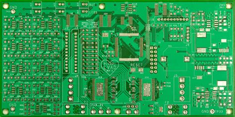
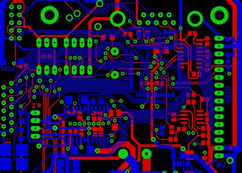
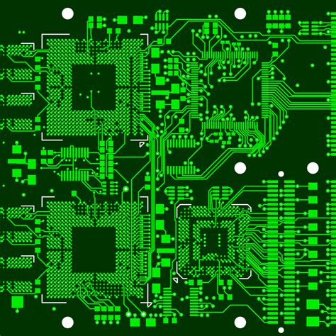
A schematic is a diagram that shows how the components in a circuit are connected electrically, without regard for the physical arrangement of the components. A PCB layout, on the other hand, shows the physical arrangement of the components on the board and the routing of the traces that connect them.
What is a design rule check (DRC)?
A design rule check (DRC) is a automated check performed by PCB design software to verify that the board layout complies with a set of design rules. These rules specify parameters such as minimum trace width, clearance between traces, via sizes, and so on. The DRC helps catch design errors early in the process, before the board is sent for manufacturing.
What is a Gerber file?
A Gerber file is a standard file format used to describe the printed circuit board layout for manufacturing. It contains information about the copper layers, solder mask, silkscreen, and drill holes. Gerber files are generated by PCB design software and sent to the PCB manufacturer for fabrication.
What is a bill of materials (BOM)?
A bill of materials (BOM) is a list of all the components used on a PCB, along with their quantities, part numbers, and other relevant information. The BOM is used by the PCB manufacturer to source the components and assemble the board. It is typically generated by the PCB design software along with the other manufacturing files.
Conclusion
PCB design, also known as printed circuit board design or PCB layout, is a critical step in the development of electronic products. It involves the process of designing and creating the layout for the copper traces, components, and features of a printed circuit board.
A well-designed PCB ensures that signals are routed correctly, power is distributed effectively, EMI is minimized, thermal management is optimized, and the board is manufacturable at scale. Poor PCB design, on the other hand, can lead to product malfunctions, reduced reliability, increased costs, and delayed time-to-market.
The PCB design process typically involves several key steps, including schematic capture, component placement, routing, design rule checking, and output generation. There are many factors that need to be considered during PCB design, such as signal integrity, power integrity, electromagnetic compatibility, thermal management, and manufacturability.
PCB design is done using specialized software tools known as EDA software, which provide a range of features and capabilities for schematic capture, component placement, routing, design rule checking, and output generation. For companies that do not have in-house PCB design expertise, there are many service providers that offer PCB design services.
By understanding the principles and best practices of PCB design, engineers can create high-quality, reliable, and manufacturable printed circuit boards that meet the needs of their products and customers.