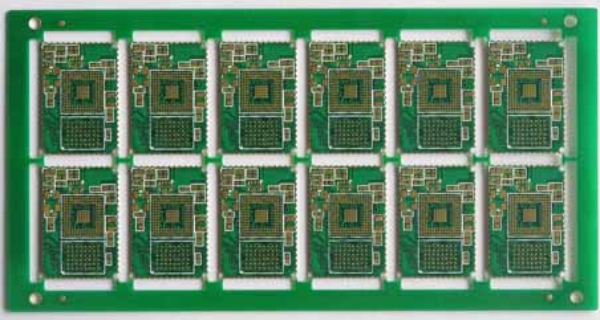
RayMing Technology NXP P89V51RD2 chip decryption program is mature, P89V51RD2 MCU decryption 100% success. In addition, we have made important breakthroughs in the field of NXP microcontroller decryption, has successfully completed a variety of models of NXP chip decryption, and our IC decryption technology have been proven over the years and repeated experiments to verify that the customer can maximize the success rate and reliability of decryption. If you have P89V51RB2 MCU decryption, P89V51RC2 MCU decryption, P89V51RD2 MCU decryption and other NXP chip cracking needs, welcome to contact: 0755-27389625!
NXP P89V51RD2 MCU Type:
p89v51rd2fa plcc44
P89V51RD2FBC TQFP44
p89v51rd2bn pdip40
NXP P89V51RD2 Microcontroller Overview:
The P89V51RD2 is an 80C51 microcontroller with 64 KB of Flash memory and 1024 bytes of data RAM.
An important feature of the P89V51RD2 is its X2 mode option. The design engineer can choose the application to run and the traditional 80C51 clock rate (12 clocks per machine cycle), or choose the X2 mode (6 clocks per machine cycle) to achieve twice the throughput at the same clock frequency. Another way to benefit from this feature
Another way to benefit from this feature is to maintain the same performance by reducing the clock frequency by half, thus greatly reducing EMI.
Flash program memory supports both parallel and serial in-system programming (ISP). The parallel programming method provides programming at high speeds, reducing programming costs and time-to-market. ISP allows device midrange products to be reprogrammed under software control. Capabilities
Field/update application firmware wide range of applications possible. the P89V51RD2 is In Application Programming (IAP), allowing reconfiguration of the Flash program memory at any time, even while the application is running.
NXP P89V51RD2 Microcontroller Features:
80C51 central processing unit
5 V operating voltage from 0 to 40 MHz
64 KB of on-chip flash program memory with ISP (in-system programming) and IAP (in-application programming)
Supports 12-clock (default) or 6-clock mode selectable via software or ISP
SPI (Serial Peripheral Interface) and Enhanced UART
PCA (Programmable Counter Array) with PWM and Capture/Compare functions.
With four 8-bit I/O ports, three high current P1 ports (16 mA each)
Three 16-bit timer/counters
Programmable Watchdog Timer (WDT)
Four prioritized 8 interrupt sources
Nth DPTR register
Low EMI mode (ALE suppression)
TTL and CMOS compatible logic levels
Undervoltage detection
Low power mode
Power-down mode, external interrupt wake-up
Idle mode
PDIP40, PLCC44 and TQFP44 packages
For P89V51RD2FA chip decryption, P89V51RD2FBC chip decryption, P89V51RD2BN chip decryption and other NXP microcontroller decryption, please look for RayMing Technology. We have low price, high success rate and fast speed for NXP chip decryption.
