
Introduction to PCB
PCB stands for Printed Circuit Board. It is a fundamental component in modern electronic devices and projects. A PCB is a flat board made of insulating material, such as fiberglass or plastic, with conductive copper traces printed on its surface. These traces connect various electronic components, such as resistors, capacitors, and integrated circuits (ICs), to form a complete electrical circuit.
History of PCBs
The concept of printed circuits dates back to the early 20th century. In 1903, Albert Hanson, a German inventor, filed a patent for a method of creating conductive patterns on an insulating substrate. However, it wasn’t until the 1940s that PCBs began to gain widespread use in electronic devices.
During World War II, the United States military heavily relied on PCBs for their electronic equipment, such as radios and radar systems. The use of PCBs allowed for more compact and reliable electronic devices, which were crucial for military applications.
After the war, PCBs became more widely adopted in consumer electronics, such as televisions and radios. As electronic devices became more complex and miniaturized, the demand for PCBs grew exponentially.
Manufacturing Process
The manufacturing process of PCBs involves several steps:
-
Design: The first step is to design the PCB layout using specialized software, such as Eagle or KiCad. The design includes the placement of components, routing of traces, and creation of ground planes.
-
Printing: Once the design is finalized, the PCB layout is printed onto a transparent film or directly onto the copper-clad board using a photoplotter.
-
Etching: The printed board is then placed in an etching solution, which removes the unwanted copper from the board, leaving only the desired traces and pads.
-
Drilling: Holes are drilled into the board for through-hole components and vias, which connect traces on different layers of the board.
-
Plating: The drilled holes are plated with copper to ensure electrical conductivity between layers.
-
Solder Mask: A solder mask is applied to the board to protect the copper traces from oxidation and to prevent accidental short circuits during soldering.
-
Silkscreen: A silkscreen layer is added to the board, which includes text and symbols to indicate component placement and other important information.
-
Assembly: Finally, the electronic components are soldered onto the board, either manually or using automated pick-and-place machines.
Types of PCBs
There are several types of PCBs, each with its own unique characteristics and applications.
Single-Layer PCBs
Single-layer PCBs, also known as single-sided PCBs, have conductive traces on only one side of the board. They are the simplest and most cost-effective type of PCB, making them ideal for low-complexity projects and prototypes.
Double-Layer PCBs
Double-layer PCBs, also known as double-sided PCBs, have conductive traces on both sides of the board. They offer more routing options and higher component density compared to single-layer PCBs. Double-layer PCBs are commonly used in more complex projects, such as consumer electronics and industrial control systems.
Multi-Layer PCBs
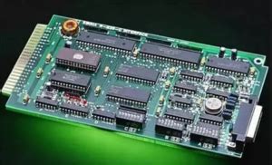
Multi-layer PCBs have three or more conductive layers, with insulating layers sandwiched between them. They offer the highest component density and routing options, making them suitable for highly complex projects, such as smartphones, computers, and aerospace applications.
| Type | Layers | Complexity | Cost | Applications |
|---|---|---|---|---|
| Single-Layer | 1 | Low | Low | Simple projects, prototypes |
| Double-Layer | 2 | Medium | Medium | Consumer electronics, control systems |
| Multi-Layer | 3+ | High | High | Smartphones, computers, aerospace |
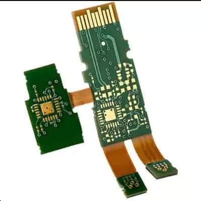
Flexible PCBs
Flexible PCBs, also known as flex circuits, are made from flexible materials, such as polyimide or PEEK. They can bend and twist without breaking, making them ideal for applications that require movement or tight spaces, such as wearable devices and automotive electronics.
Rigid-Flex PCBs
Rigid-flex PCBs combine the benefits of both rigid and flexible PCBs. They consist of rigid PCB sections connected by flexible PCB sections, allowing for three-dimensional assembly and improved reliability in high-stress applications, such as military and aerospace electronics.
PCB design Considerations
When designing a PCB, there are several important factors to consider to ensure optimal performance and reliability.
Component Placement
Proper component placement is crucial for several reasons:
-
Signal Integrity: Components should be placed in a way that minimizes the length of critical signal traces, reducing the risk of signal degradation and electromagnetic interference (EMI).
-
Thermal Management: Heat-generating components, such as power regulators and processors, should be placed in a way that allows for adequate cooling, either through natural convection or the use of heatsinks and fans.
-
Mechanical Constraints: Components should be placed in a way that allows for easy assembly and maintenance, while also considering the mechanical constraints of the enclosure or housing.
Trace Routing
Trace routing is the process of creating the conductive paths that connect components on the PCB. Proper trace routing is essential for ensuring signal integrity and minimizing EMI.
Some key considerations for trace routing include:
-
Trace Width: The width of a trace determines its current-carrying capacity and resistance. Wider traces can carry more current and have lower resistance, but they also take up more space on the board.
-
Trace Spacing: The spacing between traces determines the risk of crosstalk and EMI. Traces should be spaced far enough apart to minimize these risks, while also considering the manufacturing capabilities of the PCB fabricator.
-
Trace Length: The length of a trace determines its resistance and the risk of signal degradation. Critical signal traces should be kept as short as possible to minimize these risks.
Ground Planes
Ground planes are large areas of copper on the PCB that provide a low-impedance return path for electrical currents. They are essential for minimizing EMI and ensuring signal integrity.
When designing ground planes, it’s important to consider the following:
-
Plane Placement: Ground planes should be placed on layers adjacent to signal layers to provide a low-impedance return path for currents.
-
Plane Stitching: Ground planes on different layers should be connected together using vias, a process known as stitching, to ensure a continuous low-impedance return path.
-
Plane Splits: In some cases, it may be necessary to split a ground plane into separate sections to isolate different parts of the circuit. This can be done using a technique called slotting, which involves creating a narrow gap in the ground plane.
Electromagnetic Compatibility (EMC)
EMC refers to the ability of an electronic device to function properly in its electromagnetic environment without causing interference to other devices. PCBs play a critical role in ensuring EMC, as they can be a source of EMI if not designed properly.
Some key considerations for EMC in PCB design include:
-
Shielding: Sensitive components and traces can be shielded using metal enclosures or conductive coatings to reduce the risk of EMI.
-
Filtering: Power supply lines and other noise-sensitive traces can be filtered using capacitors and ferrite beads to reduce the risk of EMI.
-
Grounding: Proper grounding techniques, such as the use of ground planes and stitching, can help minimize EMI and ensure signal integrity.

PCB Assembly
Once the PCB design is finalized and the board is manufactured, the next step is to assemble the components onto the board. There are two main methods of PCB assembly: through-hole and surface mount.
Through-Hole Assembly
Through-hole assembly involves inserting component leads through holes drilled in the PCB and soldering them to pads on the opposite side of the board. This method is well-suited for larger components and provides a strong mechanical connection, but it requires more manual labor and takes up more space on the board compared to surface mount assembly.
Surface Mount Assembly
Surface mount assembly involves soldering components directly onto pads on the surface of the PCB. This method allows for higher component density and faster assembly compared to through-hole, but it requires more precise manufacturing techniques and specialized equipment.
| Assembly Method | Component Size | Mechanical Strength | Assembly Speed | Component Density |
|---|---|---|---|---|
| Through-Hole | Large | High | Slow | Low |
| Surface Mount | Small | Low | Fast | High |
Soldering Techniques
Soldering is the process of joining two metal surfaces using a molten metal alloy called solder. There are several soldering techniques used in PCB assembly, including:
-
Hand Soldering: This method involves manually applying solder to components and pads using a soldering iron. It is well-suited for small-scale assembly and repairs, but it is time-consuming and requires a skilled operator.
-
Wave Soldering: This method involves passing the PCB over a wave of molten solder, which selectively solders components to the board. It is well-suited for through-hole assembly and provides a fast and efficient way to solder multiple components at once.
-
Reflow Soldering: This method involves applying solder paste to the PCB pads and placing components onto the paste. The board is then heated in a reflow oven, which melts the solder and secures the components to the board. It is well-suited for surface mount assembly and provides a fast and efficient way to solder multiple components at once.
PCB Testing and Inspection
After assembly, PCBs must be thoroughly tested and inspected to ensure they meet the required specifications and performance criteria. There are several methods of PCB testing and inspection, including:
Visual Inspection
Visual inspection involves examining the PCB for defects such as solder bridges, cold solder joints, and component misalignment. This can be done manually using a microscope or automated using machine vision systems.
Automated Optical Inspection (AOI)
AOI uses cameras and image processing algorithms to automatically detect defects on the PCB. It is faster and more accurate than manual visual inspection and can detect defects that are difficult to see with the naked eye.
In-Circuit Testing (ICT)
ICT involves using a bed-of-nails fixture to make electrical contact with specific points on the PCB and measuring the electrical characteristics of the circuit. This allows for detailed testing of individual components and connections, but it requires a custom fixture for each PCB design.
Functional Testing
Functional testing involves applying power to the PCB and testing its functionality under real-world operating conditions. This can be done using specialized test equipment or by integrating the PCB into the final product and testing it as part of the overall system.
| Testing Method | Defects Detected | Speed | Accuracy | Cost |
|---|---|---|---|---|
| Visual Inspection | Solder bridges, cold joints | Slow | Low | Low |
| Automated Optical Inspection | Solder defects, component placement | Fast | High | Medium |
| In-Circuit Testing | Component and connection faults | Medium | High | High |
| Functional Testing | Overall system functionality | Slow | High | Medium |
Conclusion
PCBs are an essential component in modern electronic devices and projects. They provide a reliable and efficient way to interconnect electronic components and form complete electrical circuits. Understanding the different types of PCBs, design considerations, assembly methods, and testing techniques is crucial for anyone involved in electronic product development.
As electronic devices continue to become more complex and miniaturized, the demand for high-quality PCBs will only continue to grow. By staying up-to-date with the latest PCB technologies and best practices, engineers and designers can create innovative and reliable electronic products that meet the needs of today’s rapidly evolving market.
FAQ
- What are the advantages of using PCBs in electronic projects?
-
PCBs offer several advantages, including:
- Compact and efficient packaging of electronic components
- Reliable and consistent electrical connections
- Improved signal integrity and reduced electromagnetic interference
- Simplified assembly and manufacturing processes
- Reduced overall system cost and improved reliability
-
What software is used for PCB design?
-
There are several software options available for PCB design, including:
- Autodesk Eagle
- KiCad
- Altium Designer
- Cadence OrCAD
- Mentor Graphics PADS
-
What are the different types of PCB materials?
-
The most common PCB materials include:
- FR-4: A composite material made of fiberglass and epoxy resin, widely used for its good mechanical and electrical properties
- Polyimide: A flexible material used for flex circuits and high-temperature applications
- Ceramic: Used for high-frequency and high-power applications due to its excellent thermal and dielectric properties
- Aluminum: Used for heat dissipation in power electronics applications
-
What is the difference between through-hole and surface mount assembly?
- Through-hole assembly involves inserting component leads through holes drilled in the PCB and soldering them to pads on the opposite side of the board. It offers strong mechanical connections but requires more manual labor and takes up more space.
-
Surface mount assembly involves soldering components directly onto pads on the surface of the PCB. It allows for higher component density and faster assembly but requires more precise manufacturing techniques and specialized equipment.
-
What are the key considerations for PCB testing and inspection?
- The key considerations for PCB testing and inspection include:
- Detecting manufacturing defects such as solder bridges, cold solder joints, and component misalignment
- Verifying the electrical characteristics of individual components and connections
- Ensuring the overall functionality and performance of the PCB under real-world operating conditions
- Choosing the appropriate testing methods based on the complexity and requirements of the PCB design
- Balancing the cost, speed, and accuracy of different testing methods to optimize the overall manufacturing process.