Judy@4pcba.com
7:30 AM - 7:30 PM
Monday to Saturday

Archive: March 15, 2024

What is PCB in aircraft?

Introduction

Printed Circuit Boards (PCBs) are an essential component in modern aircraft, enabling the complex electronic systems that power everything from navigation and communication to engine control and in-flight entertainment. In this comprehensive guide, we’ll explore the role of PCBs in aviation, their design and manufacturing process, and the unique challenges and regulations associated with their use in aircraft.

What are Printed Circuit Boards?

Definition and Components

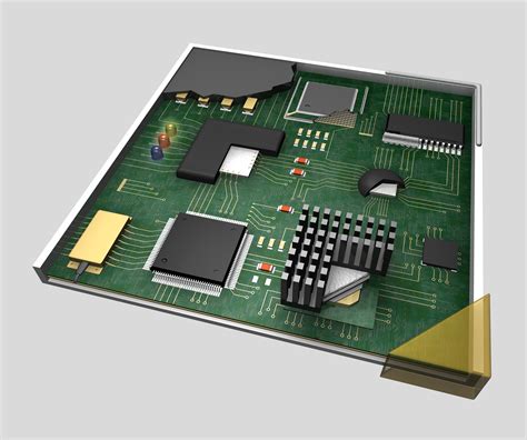
A Printed Circuit Board (PCB) is a thin board made of insulating material, such as fiberglass or composite, with conductive copper traces etched onto its surface. These traces connect various electronic components, such as resistors, capacitors, and integrated circuits (ICs), to form a complete electronic circuit.

The main components of a PCB include:

  • Substrate: The insulating board that provides mechanical support and electrical insulation
  • Copper traces: Conductive pathways that connect components
  • Solder mask: A protective layer that prevents short circuits and corrosion
  • Silkscreen: Text and symbols printed on the board for identification and assembly
  • Electronic components: The various parts that make up the circuit, such as resistors, capacitors, and ICs
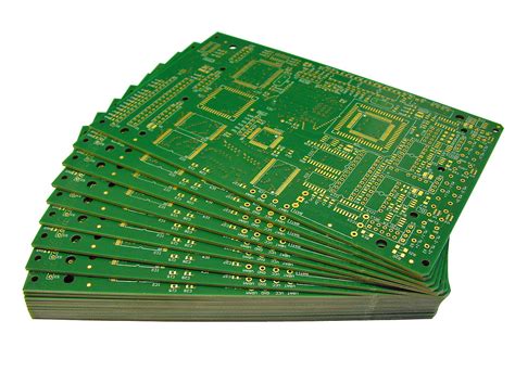
Types of PCBs

PCBs can be classified based on the number of conductive layers they contain:

  1. Single-sided PCBs: These have copper traces on only one side of the substrate and are suitable for simple, low-density circuits.
  2. Double-sided PCBs: With copper traces on both sides of the substrate, these boards offer higher component density and more complex routing options.
  3. Multi-layer PCBs: These consist of multiple layers of conductive traces separated by insulating layers, allowing for even higher component density and more complex circuits. Multi-layer PCBs are commonly used in aircraft electronics.

The Role of PCBs in Aircraft

Avionics and Flight Control Systems

PCBs are the backbone of an aircraft’s avionics and flight control systems, which include:

  • Navigation systems: GPS, INS, and radio navigation
  • Communication systems: Radios, transponders, and data links
  • Autopilot and flight management systems
  • Instrument displays and control panels

These systems rely on high-performance PCBs to process data, communicate with other systems, and provide reliable operation in the demanding environment of an aircraft.

Engine Control and Monitoring

Modern aircraft engines are controlled and monitored by Electronic Engine Control (EEC) systems, which use PCBs to:

  • Regulate fuel flow and ignition timing
  • Monitor engine parameters such as temperature, pressure, and vibration
  • Communicate with other aircraft systems and ground-based maintenance computers

The PCBs in these systems must be designed to withstand the high temperatures, vibrations, and electromagnetic interference (EMI) present in an aircraft engine environment.

In-Flight Entertainment and Cabin Systems

PCBs also play a crucial role in an aircraft’s passenger cabin, powering systems such as:

  • In-flight entertainment (IFE) systems: Displays, audio systems, and content servers
  • Cabin lighting and environmental control systems
  • Passenger service units (PSUs) and call buttons
  • Seat electronics, including power outlets and USB ports

These systems require PCBs that are lightweight, compact, and reliable, with the ability to interface with a variety of peripheral devices and networks.

PCB design and Manufacturing for Aircraft

Design Considerations

Designing PCBs for use in aircraft presents several unique challenges, including:

  • Environmental factors: PCBs must be able to withstand extreme temperatures, humidity, vibration, and altitude changes.
  • EMI and EMC: Aircraft electronics must not interfere with each other or with external systems, requiring careful design for electromagnetic compatibility (EMC).
  • Size and weight constraints: PCBs must be as small and lightweight as possible to minimize their impact on aircraft performance and fuel efficiency.
  • Reliability and redundancy: Aircraft systems require high levels of reliability and often incorporate redundant components and circuits to ensure continuous operation.

To address these challenges, PCB designers use specialized software tools and follow industry standards and guidelines, such as RTCA DO-160 and ARINC 600.

Manufacturing Process

The manufacturing process for aircraft PCBs involves several key steps:

  1. PCB design: The circuit is designed using CAD software, and the layout is optimized for manufacturability and performance.
  2. Fabrication: The bare PCB is manufactured using a multi-step process that includes:
  3. Creating the substrate
  4. Applying and patterning the copper layers
  5. Drilling holes and vias
  6. Applying solder mask and silkscreen
  7. Assembly: Electronic components are mounted onto the PCB using automated pick-and-place machines and soldered in place using reflow ovens or wave soldering.
  8. Testing and inspection: The assembled PCB undergoes rigorous testing and inspection to ensure it meets the required specifications and quality standards.

Throughout the manufacturing process, strict quality control measures are in place to ensure the PCBs meet the high reliability and performance requirements of the aviation industry.

Quality and Reliability Standards

PCBs used in aircraft must meet stringent quality and reliability standards to ensure the safety and performance of the aircraft. Some of the key standards and certifications include:

  • RTCA DO-254: Design Assurance Guidance for Airborne Electronic Hardware
  • RTCA DO-160: Environmental Conditions and Test Procedures for Airborne Equipment
  • ARINC 600: Air Transport Avionics Equipment Interfaces
  • AS9100: Quality Management Systems – Requirements for Aviation, Space, and Defense Organizations

Manufacturers of aircraft PCBs must demonstrate compliance with these standards through rigorous testing, documentation, and auditing processes.

Challenges and Future Trends

Environmental and Regulatory Challenges

The use of PCBs in aircraft presents several environmental and regulatory challenges, including:

  • Hazardous materials: Some PCB manufacturing processes involve hazardous chemicals, such as lead and halogenated flame retardants, which are subject to increasingly strict regulations.
  • Waste management: The disposal of end-of-life PCBs and electronic waste is a growing concern, requiring responsible recycling and waste management practices.
  • Greenhouse gas emissions: The energy-intensive manufacturing process and the use of certain materials can contribute to greenhouse gas emissions, prompting the industry to explore more sustainable practices.

To address these challenges, the aviation industry is working to develop and adopt more environmentally friendly materials and processes, such as lead-free solders and halogen-free flame retardants.

Emerging Technologies and Trends

The future of PCBs in aircraft is shaped by several emerging technologies and trends, including:

  • Additive manufacturing: 3D printing techniques, such as inkjet and aerosol jet printing, offer new possibilities for creating complex, lightweight PCBs with embedded components.
  • Flexible and stretchable electronics: The development of flexible and stretchable PCB materials and components enables the integration of electronics into non-traditional aircraft structures, such as wings and fuselages.
  • Wireless technologies: The increasing use of wireless communication and power transfer technologies, such as Bluetooth and inductive coupling, may reduce the need for physical PCB Connections in some applications.
  • Modular and reconfigurable systems: The trend towards modular and reconfigurable aircraft systems may lead to the development of more standardized and interchangeable PCBs, facilitating maintenance and upgrades.

As these technologies mature, they are likely to have a significant impact on the design, manufacturing, and performance of PCBs in aircraft.

Frequently Asked Questions (FAQ)

  1. Q: What is the difference between a PCB and a circuit board?
    A: “PCB” and “circuit board” are often used interchangeably, as a PCB is a type of circuit board. However, “circuit board” can also refer to other types of boards, such as breadboards or stripboards, which are used for prototyping or low-volume production.

  2. Q: Why are multi-layer PCBs commonly used in aircraft?
    A: Multi-layer PCBs are used in aircraft because they offer several advantages, including higher component density, more complex routing options, and better EMI/EMC performance. These features are essential for the compact, high-performance electronic systems found in modern aircraft.

  3. Q: How do aircraft PCBs differ from those used in other industries?
    A: Aircraft PCBs are designed and manufactured to meet the unique challenges of the aviation environment, such as extreme temperatures, vibration, and altitude changes. They also must comply with strict quality and reliability standards specific to the aerospace industry, such as RTCA DO-160 and ARINC 600.

  4. Q: What materials are used to make PCBs for aircraft?
    A: PCBs for aircraft are typically made from high-performance materials, such as polyimide, PTFE, or high-temperature epoxy laminates. These materials offer excellent thermal stability, mechanical strength, and chemical resistance, making them suitable for the demanding conditions found in aircraft.

  5. Q: How are PCBs in aircraft tested to ensure reliability?
    A: PCBs used in aircraft undergo rigorous testing to ensure they meet the required quality and reliability standards. This includes environmental testing (e.g., temperature, humidity, and vibration), EMI/EMC testing, and functional testing. Additionally, manufacturers must follow strict quality control processes and maintain detailed documentation to demonstrate compliance with industry standards.

Conclusion

Printed Circuit Boards play a critical role in enabling the complex electronic systems that power modern aircraft. From avionics and flight control to engine management and in-flight entertainment, PCBs are essential for ensuring the safety, efficiency, and comfort of air travel.

Designing and manufacturing PCBs for aircraft presents unique challenges, requiring specialized materials, processes, and quality standards to meet the demanding requirements of the aviation industry. As new technologies and trends emerge, the role of PCBs in aircraft will continue to evolve, driving innovation and shaping the future of aviation electronics.

By understanding the importance of PCBs in aircraft and the challenges associated with their design and manufacture, we can appreciate the vital role they play in keeping our skies safe and our aircraft at the forefront of technological advancement.

How do you reverse engineer a PCB from an image?

What is PCB reverse engineering?

PCB reverse engineering is the process of analyzing an existing printed circuit board to understand its design, functionality, and components. This process involves creating a schematic diagram and a bill of materials (BOM) based on the information gathered from the PCB image. Reverse engineering a PCB can be useful in various scenarios, such as:

  • Repairing or modifying an existing PCB when the original design files are unavailable
  • Analyzing a competitor’s product to understand its functionality and design
  • Learning from existing designs to improve one’s own PCB design skills

Tools required for PCB reverse engineering

To successfully reverse engineer a PCB from an image, you will need the following tools:

  1. High-resolution camera or scanner
  2. Image editing software (e.g., Adobe Photoshop, GIMP)
  3. PCB design software (e.g., Altium Designer, KiCad, Eagle)
  4. Magnifying glass or microscope
  5. Multimeter
  6. Soldering iron and desoldering tools

Step-by-step guide to reverse engineering a PCB from an image

Step 1: Capture a high-quality image of the PCB

The first step in reverse engineering a PCB is to obtain a clear, high-resolution image of both sides of the board. You can use a high-quality digital camera or a scanner to capture the images. Ensure that the images are well-lit, in focus, and free from any distortions or reflections.

Tips for capturing a high-quality PCB image:
– Use a tripod to minimize camera shake
– Ensure proper lighting to avoid shadows and reflections
– Capture multiple images with different exposure settings to get the best possible result
– If using a scanner, place a dark background behind the PCB to improve contrast

Step 2: Clean up the PCB image

Once you have captured the images, use image editing software to clean them up. This process involves adjusting the brightness, contrast, and color balance to enhance the visibility of the PCB traces, components, and labels. You may also need to remove any background noise or artifacts that could interfere with the analysis process.

Image editing techniques for PCB cleanup:
– Adjust levels and curves to improve contrast
– Use the clone stamp tool to remove any dust, scratches, or unwanted artifacts
– Apply sharpening filters to enhance the clarity of traces and component outlines
– Use color adjustment tools to improve the visibility of different layers (e.g., solder mask, silkscreen)

Step 3: Identify components and their values

With the cleaned-up PCB images, begin identifying the components on the board. Use a magnifying glass or microscope to read the component labels and markings. Note down the component types (e.g., resistors, capacitors, ICs) and their values (e.g., resistance, capacitance, part numbers). If some components are not labeled, you may need to use a multimeter to measure their values or research their appearance online.

Common components and their identification:
– Resistors: Labeled with color codes or numerical values
– Capacitors: Labeled with capacitance and voltage ratings
– Inductors: Labeled with inductance values
– ICs: Labeled with part numbers, which can be searched in online databases
– Connectors: Identified by their type (e.g., USB, HDMI, power) and number of pins

Step 4: Trace the PCB Connections

Once you have identified the components, the next step is to trace the connections between them. Start by identifying the power and ground connections, as these are usually the most prominent traces on the board. Then, follow the traces from each component pin to determine their connections to other components.

Tips for tracing PCB connections:
– Use the continuity function of a multimeter to verify connections between points
– Pay attention to via holes, as they indicate connections between layers
– Use PCB design software to create a schematic diagram while tracing the connections
– Cross-reference the traced connections with the component datasheets to ensure accuracy

Step 5: Create a schematic diagram

As you trace the connections, create a schematic diagram using PCB design software. The schematic diagram is a graphical representation of the electrical connections between components, using standardized symbols for each component type. Ensure that the schematic is well-organized, with components grouped by their function and labeled clearly.

Best practices for creating a PCB schematic:
– Use a consistent naming convention for components and nets
– Group related components together (e.g., power supply, microcontroller, sensors)
– Use net labels to clarify the purpose of each connection
– Add notes and comments to explain the function of specific components or circuits
– Verify the schematic against the traced connections to ensure accuracy

Step 6: Generate a bill of materials (BOM)

With the schematic diagram complete, create a bill of materials (BOM) that lists all the components used in the PCB. The BOM should include the following information for each component:

  • Reference designator (e.g., R1, C2, U3)
  • Component type (e.g., resistor, capacitor, IC)
  • Value or part number
  • Package type (e.g., 0805, SOIC-8)
  • Manufacturer and supplier information (if available)

The BOM is essential for sourcing components if you plan to reproduce the PCB or repair the original board.

Step 7: Validate the reverse-engineered design

Before considering the reverse engineering process complete, validate the schematic and BOM against the original PCB. This involves comparing the traced connections and component placements with the actual board, looking for any discrepancies or errors. You may also want to research the functionality of the PCB based on the identified components and their datasheets to ensure that the reverse-engineered design is accurate and complete.

Validation techniques:
– Visual inspection of the PCB and schematic side-by-side
– Continuity testing of the PCB connections using a multimeter
– Functional testing of the PCB (if possible) to verify its operation
– Cross-referencing component datasheets with the schematic and BOM

Challenges in PCB reverse engineering

Reverse engineering a PCB from an image can be a challenging process due to several factors:

  1. Component identification: Some components may have unclear or missing markings, making it difficult to determine their values or part numbers.

  2. Multilayer boards: PCBs with multiple layers can be challenging to reverse engineer, as the connections between layers may not be visible in the images.

  3. High-density designs: PCBs with high component density or fine-pitch traces can be difficult to trace accurately, requiring high-resolution images and precise analysis.

  4. Damaged or modified boards: If the original PCB is damaged or has been modified, it may be difficult to determine the original design intent or functionality.

  5. Intellectual property concerns: Reverse engineering a PCB may raise intellectual property concerns, especially if the design is protected by patents or trade secrets.

Best practices for PCB reverse engineering

To overcome these challenges and ensure a successful reverse engineering process, consider the following best practices:

  1. Use high-quality images: Invest in a good camera or scanner to capture clear, high-resolution images of the PCB.

  2. Work methodically: Follow a systematic approach to component identification and connection tracing, double-checking your work as you progress.

  3. Use appropriate tools: Employ PCB design software, multimeters, and magnification tools to aid in the analysis process.

  4. Collaborate with others: If possible, work with a team of experienced PCB designers or engineers to share knowledge and insights.

  5. Document your work: Keep detailed notes, schematics, and BOMs throughout the reverse engineering process to ensure accuracy and reproducibility.

  6. Respect intellectual property: Be aware of any legal or ethical considerations related to reverse engineering, and ensure that you have the necessary permissions or rights to analyze the PCB design.

FAQ

  1. What is the purpose of reverse engineering a PCB?
    Reverse engineering a PCB can be done for various reasons, such as repairing or modifying an existing board, analyzing a competitor’s product, or learning from existing designs to improve one’s own PCB design skills.

  2. What tools do I need to reverse engineer a PCB from an image?
    To reverse engineer a PCB from an image, you will need a high-resolution camera or scanner, image editing software, PCB design software, a magnifying glass or microscope, a multimeter, and soldering tools.

  3. How do I identify components on a PCB?
    Components can be identified by their markings, labels, or physical appearance. Resistors and capacitors are often labeled with color codes or numerical values, while ICs have part numbers that can be searched in online databases. If components are not labeled, you may need to measure their values using a multimeter or research their appearance online.

  4. What should I do if the PCB has multiple layers?
    Multilayer PCBs can be challenging to reverse engineer, as the connections between layers may not be visible in the images. In such cases, you may need to rely on continuity testing using a multimeter and cross-referencing component datasheets to determine the connections between layers.

  5. Are there any legal or ethical considerations when reverse engineering a PCB?
    Yes, reverse engineering a PCB may raise intellectual property concerns, especially if the design is protected by patents or trade secrets. It is essential to ensure that you have the necessary permissions or rights to analyze the PCB design and to be aware of any legal or ethical considerations related to reverse engineering.

Conclusion

Reverse engineering a PCB from an image is a complex process that requires a combination of technical skills, specialized tools, and attention to detail. By following a systematic approach and employing best practices, you can successfully analyze an existing PCB design and create an accurate schematic diagram and bill of materials.

Remember to work methodically, use high-quality images, and collaborate with others when possible to overcome the challenges associated with PCB reverse engineering. Additionally, be mindful of any legal or ethical considerations related to analyzing and reproducing existing designs.

By mastering the art of PCB reverse engineering, you can gain valuable insights into the design and functionality of electronic products, enabling you to repair, modify, or learn from existing PCBs. This skill can be particularly useful for engineers, technicians, and hobbyists working in the electronics industry or pursuing personal projects.

How can we protect PCB from reverse engineering?

Introduction to PCB Protection

Printed Circuit Boards (PCBs) are the backbone of modern electronic devices. They contain critical information about the design and functionality of the device, making them a prime target for reverse engineering. Reverse engineering of PCBs can lead to intellectual property theft, counterfeiting, and even security breaches. Therefore, it is essential to protect PCBs from reverse engineering to safeguard the device’s integrity and the manufacturer’s intellectual property.

In this article, we will explore various techniques and methods to protect PCBs from reverse engineering. We will discuss the importance of PCB protection, the risks associated with reverse engineering, and the best practices to prevent unauthorized access to PCB design information.

Understanding Reverse Engineering

Reverse engineering is the process of analyzing a device or system to understand its design, functionality, and components. In the context of PCBs, reverse engineering involves studying the board’s layout, components, and connections to extract information about the device’s operation and design.

Reverse engineering can be performed for various reasons, including:

  1. Competitive analysis
  2. Debugging and troubleshooting
  3. Counterfeit product detection
  4. Intellectual property theft

While reverse engineering can be a legitimate practice in some cases, such as for educational or research purposes, it can also be used maliciously to copy designs, create counterfeit products, or gain unauthorized access to sensitive information.

Risks Associated with PCB Reverse Engineering

PCB reverse engineering poses several risks to manufacturers and device owners, including:

  1. Intellectual Property Theft: Reverse engineering can expose the proprietary design and functionality of a device, allowing competitors to copy or improve upon the original design without investing in research and development.

  2. Counterfeiting: Counterfeiters can use the information obtained from reverse engineering to create fake products that look and function like the original, leading to lost revenue and damage to the manufacturer’s reputation.

  3. Security Breaches: In some cases, reverse engineering can reveal sensitive information about the device’s security features, such as encryption keys or authentication mechanisms, making the device vulnerable to attacks.

  4. Loss of Competitive Advantage: If a competitor gains access to a company’s proprietary PCB designs, they can use that information to develop similar or improved products, eroding the original manufacturer’s competitive edge.

Techniques for PCB Protection

There are several techniques and methods that manufacturers can employ to protect their PCBs from reverse engineering. These include:

1. Obfuscation

Obfuscation is the process of making the PCB design more difficult to understand and analyze. This can be achieved through various means, such as:

  • Using complex routing patterns
  • Hiding critical components under other components or potting material
  • Using blind or buried vias to conceal connections
  • Employing multi-layer boards with inner layers dedicated to security

By making the PCB design more complex and harder to decipher, obfuscation can deter potential reverse engineers and increase the time and effort required to extract useful information from the board.

2. Encryption

Encryption involves using mathematical algorithms to convert plain text or data into a coded format that can only be deciphered with the correct encryption key. In the context of PCB protection, encryption can be used to secure sensitive data stored on the board, such as firmware or configuration settings.

Some common encryption techniques used in PCBs include:

  • Advanced Encryption Standard (AES)
  • Rivest-Shamir-Adleman (RSA)
  • Elliptic Curve Cryptography (ECC)

By encrypting sensitive data, manufacturers can prevent unauthorized access to the device’s functionality and protect against intellectual property theft.

3. Tamper Detection and Response

Tamper detection and response mechanisms are designed to detect and respond to unauthorized attempts to access or modify the PCB. These mechanisms can include:

  • Tamper-evident seals or coatings that show signs of tampering
  • Tamper switches that detect physical intrusion and trigger a response
  • Active shield layers that detect and respond to drilling or probing attempts
  • Self-destructing components that render the PCB inoperable if tampered with

When a tamper event is detected, the PCB can respond by erasing sensitive data, disabling critical functions, or even physically destroying key components to prevent further unauthorized access.

4. Secure Boot and Firmware Validation

Secure boot and firmware validation techniques ensure that the device only runs authentic and unmodified firmware. This can be achieved through:

  • Digital signatures that verify the authenticity and integrity of the firmware
  • Secure boot processes that validate the firmware before execution
  • Secure firmware update mechanisms that prevent unauthorized modifications

By implementing secure boot and firmware validation, manufacturers can prevent attackers from replacing the original firmware with malicious or counterfeit versions, protecting the device’s integrity and functionality.

5. Physical Security Measures

Physical security measures aim to prevent unauthorized physical access to the PCB. These can include:

  • Tamper-resistant enclosures that prevent opening or removal of the PCB
  • Potting or encapsulation of critical components to prevent physical access
  • Use of special screws or fasteners that require proprietary tools for removal
  • Implementing sensors that detect and respond to physical tampering attempts

By making it difficult or impossible to physically access the PCB, manufacturers can deter reverse engineering attempts and protect the device’s sensitive components.

Best Practices for PCB Protection

To effectively protect PCBs from reverse engineering, manufacturers should follow these best practices:

  1. Conduct a Threat Analysis: Identify the potential risks and threats to the PCB, considering factors such as the device’s intended use, the sensitivity of the data it handles, and the potential consequences of reverse engineering.

  2. Implement a Multi-Layered Approach: Use a combination of obfuscation, encryption, tamper detection, secure boot, and physical security measures to create a comprehensive protection strategy.

  3. Regularly Update and Patch Firmware: Keep the device’s firmware up to date with the latest security patches and updates to address any vulnerabilities that may be discovered over time.

  4. Educate Employees and Partners: Train employees and partners on the importance of PCB protection and the best practices for handling sensitive information and devices.

  5. Monitor and Audit: Regularly monitor the device’s security posture and conduct audits to identify and address any weaknesses or breaches in the protection mechanisms.

By following these best practices and implementing a robust PCB protection strategy, manufacturers can significantly reduce the risk of reverse engineering and safeguard their intellectual property and sensitive information.

Frequently Asked Questions (FAQ)

  1. What is PCB reverse engineering?
    PCB reverse engineering is the process of analyzing a printed circuit board to understand its design, functionality, and components without access to the original design documents or schematics.

  2. Why is PCB protection important?
    PCB protection is crucial to prevent intellectual property theft, counterfeiting, and security breaches that can result from reverse engineering. By safeguarding the PCB design and sensitive information, manufacturers can maintain their competitive advantage and ensure the integrity of their devices.

  3. What are some common techniques used for PCB protection?
    Common techniques for PCB protection include obfuscation, encryption, tamper detection and response, secure boot and firmware validation, and physical security measures. These techniques aim to make the PCB more difficult to reverse engineer and protect sensitive data and functionality.

  4. Can PCB protection guarantee complete security against reverse engineering?
    While PCB protection techniques can significantly reduce the risk of reverse engineering, no protection method is foolproof. Determined attackers with sufficient resources and expertise may still be able to reverse engineer a protected PCB given enough time and effort. However, implementing a comprehensive protection strategy can make the process much more difficult and deter most reverse engineering attempts.

  5. How can manufacturers balance PCB protection with maintainability and debugging?
    Manufacturers can balance PCB protection with maintainability and debugging by implementing protection mechanisms that can be selectively disabled or bypassed by authorized personnel. This can be achieved through secure authentication methods, such as hardware security tokens or secure debug interfaces. Additionally, manufacturers can provide limited access to diagnostic tools and information to authorized service centers while still maintaining a high level of protection against unauthorized access.

Conclusion

Protecting PCBs from reverse engineering is a critical aspect of ensuring the security and integrity of electronic devices. By understanding the risks associated with reverse engineering and implementing a comprehensive protection strategy that includes obfuscation, encryption, tamper detection, secure boot, and physical security measures, manufacturers can safeguard their intellectual property and prevent unauthorized access to sensitive information.

As the threat landscape continues to evolve, it is essential for manufacturers to stay informed about the latest PCB protection techniques and best practices. By regularly updating and auditing their protection mechanisms, manufacturers can maintain a strong security posture and minimize the risk of reverse engineering.

Ultimately, PCB protection is an ongoing process that requires collaboration among designers, engineers, and security experts to create robust and effective solutions that balance security, functionality, and maintainability. By prioritizing PCB protection, manufacturers can ensure the long-term success and integrity of their electronic devices in an increasingly competitive and risky market.

How is a PCB protected after manufacture?

The Importance of PCB protection

PCBs are subjected to a wide range of environmental stresses, including temperature fluctuations, humidity, dust, and chemical exposure. These factors can lead to corrosion, short circuits, and other issues that compromise the integrity of the PCB and the overall performance of the electronic device. Moreover, during handling and assembly, PCBs are susceptible to physical damage such as scratches, dents, and static discharge. Therefore, implementing proper PCB protection measures is essential to mitigate these risks and extend the lifespan of the PCB.

Conformal Coating

One of the most common and effective methods of PCB protection is conformal coating. Conformal coating involves applying a thin, protective layer of material over the surface of the PCB, including its components and solder joints. This coating acts as a barrier against moisture, dust, chemicals, and other contaminants, preventing them from reaching the sensitive electronics on the board.

Types of Conformal Coatings

There are several types of conformal coatings available, each with its own unique properties and advantages:

  1. Acrylic Resin: Acrylic coatings offer excellent moisture and fungal resistance, making them suitable for high-humidity environments. They are easy to apply and remove, making repairs and modifications convenient.

  2. Silicone Resin: Silicone coatings provide superior protection against extreme temperatures and UV exposure. They are highly flexible and have excellent dielectric properties, making them ideal for high-voltage applications.

  3. Polyurethane Resin: Polyurethane coatings offer a balance of moisture resistance, mechanical strength, and chemical resistance. They are abrasion-resistant and provide good protection against solvents and oils.

  4. Epoxy Resin: Epoxy coatings are known for their excellent chemical resistance and mechanical strength. They provide a hard, durable finish that is suitable for harsh industrial environments.

  5. Parylene: Parylene is a vapor-deposited polymer coating that offers exceptional conformality and uniform coverage. It provides excellent barrier properties against moisture and chemicals while being ultra-thin and lightweight.

Conformal Coating Application Methods

Conformal coatings can be applied using various methods, depending on the specific requirements of the PCB and the production volume:

  1. Brushing: Manual brushing is suitable for low-volume production or touch-up applications. It allows for precise control but can be time-consuming and may result in inconsistent coating thickness.

  2. Spraying: Spray coating is a popular choice for high-volume production. It offers fast and efficient coverage but may require masking of areas that do not require coating.

  3. Dipping: Dip coating involves immersing the PCB in a bath of coating material. It provides excellent coverage and is suitable for complex geometries but may require longer drying times.

  4. Selective Coating: Selective coating techniques, such as needle dispensing or robotic dispensing, allow for precise application of the coating material only on specific areas of the PCB. This method is ideal for PCBs with components that are sensitive to coating or require selective protection.

Coating Type Moisture Resistance Temperature Range Chemical Resistance Dielectric Strength Ease of Application
Acrylic Excellent -55°C to 125°C Good Good Easy
Silicone Excellent -65°C to 200°C Good Excellent Moderate
Polyurethane Very Good -55°C to 125°C Very Good Good Moderate
Epoxy Good -55°C to 150°C Excellent Very Good Difficult
Parylene Excellent -200°C to 200°C Excellent Very Good Specialized

Encapsulation

Encapsulation is another method of PCB protection that involves completely sealing the PCB and its components within a protective material. This method provides a higher level of protection compared to conformal coating, as it creates a solid barrier against environmental factors and physical damage.

Encapsulation Materials

Various materials can be used for PCB encapsulation, each with its own properties and advantages:

  1. Potting Compounds: Potting compounds are liquid polymers that are poured over the PCB and allowed to cure, forming a solid protective layer. Common potting materials include epoxy, silicone, and polyurethane. They provide excellent moisture resistance, mechanical strength, and thermal insulation.

  2. Overmolding: Overmolding involves injecting a thermoplastic or thermoset material around the PCB, creating a seamless protective enclosure. This method is suitable for high-volume production and offers a high degree of design flexibility, allowing for the integration of features such as connectors and mounting points.

  3. Transfer Molding: Transfer molding is similar to overmolding but uses a preheated molding compound that is transferred into a mold cavity containing the PCB. This method is suitable for high-volume production and offers excellent dimensional stability and consistency.

Encapsulation Design Considerations

When designing an encapsulated PCB, several factors need to be considered to ensure optimal protection and functionality:

  1. Material Selection: The encapsulation material should be chosen based on the specific requirements of the application, such as temperature range, chemical resistance, and mechanical properties.

  2. Thermal Management: Encapsulation can impact the thermal dissipation of the PCB, so proper thermal management techniques, such as the use of heat sinks or thermal vias, should be incorporated into the design.

  3. Stress Relief: The encapsulation process can introduce mechanical stresses on the PCB and its components. Stress relief features, such as flexible leads or elastomeric pads, should be incorporated to minimize the risk of damage.

  4. Serviceability: Encapsulated PCBs are typically more difficult to repair or modify compared to conformal coated PCBs. The design should consider the need for serviceability and incorporate features such as removable covers or access points if necessary.

Solder Mask

Solder mask, also known as solder resist, is a thin, protective layer applied to the copper traces on a PCB. Its primary purpose is to prevent solder bridging and short circuits during the soldering process, but it also provides a degree of protection against environmental factors.

Solder Mask Materials

Solder masks are typically made from polymer materials that are resistant to heat, chemicals, and moisture. The most common types of solder mask materials are:

  1. Liquid Photoimageable Solder Mask (LPISM): LPISM is a photosensitive polymer that is applied as a liquid and then exposed to UV light through a photographic film. The exposed areas cure and become resistant to the developer solution, while the unexposed areas are washed away, leaving a patterned solder mask layer.

  2. Dry Film Solder Mask (DFSM): DFSM is a solid film that is laminated onto the PCB surface and then exposed to UV light through a photographic film. The exposed areas cure and become resistant to the developer solution, while the unexposed areas are removed, leaving a patterned solder mask layer.

Solder Mask Application Process

The solder mask application process typically involves the following steps:

  1. Surface Preparation: The PCB surface is cleaned and roughened to improve the adhesion of the solder mask.

  2. Solder Mask Application: The solder mask material is applied to the PCB surface, either as a liquid (LPISM) or a film (DFSM).

  3. Exposure: The solder mask is exposed to UV light through a photographic film, which defines the desired pattern.

  4. Development: The unexposed areas of the solder mask are removed using a developer solution, leaving a patterned solder mask layer.

  5. Curing: The solder mask is cured using heat or UV light to improve its mechanical and chemical properties.

Solder Mask Design Considerations

When designing a solder mask for a PCB, several factors need to be considered:

  1. Solder Mask Color: Solder masks are available in various colors, with green being the most common. The choice of color can impact the visibility of the PCB features and the aesthetics of the final product.

  2. Solder Mask Thickness: The thickness of the solder mask can impact its protective properties and the ease of soldering. A typical solder mask thickness ranges from 0.5 to 2 mils (0.0127 to 0.0508 mm).

  3. Solder Mask Clearance: The solder mask should be designed with appropriate clearances around pads, vias, and other features to ensure proper solderability and prevent solder bridging.

  4. Solder Mask Compatibility: The solder mask material should be compatible with the PCB substrate, the soldermask, and the assembly process to ensure optimal adhesion and performance.

Solder Mask Type Thickness Range (mils) UV Exposure Required Compatibility
LPISM 0.5 – 2.0 Yes Epoxy, Polyimide, FR-4
DFSM 0.5 – 2.0 Yes Epoxy, Polyimide, FR-4

PCB Handling and Storage

Proper handling and storage of PCBs are critical to maintaining their protective layers and ensuring their long-term reliability. Some best practices for PCB handling and storage include:

  1. ESD Protection: PCBs should be handled in an ESD-safe environment, using appropriate ESD protection equipment such as grounded workstations, wrist straps, and ESD-safe packaging materials.

  2. Clean Environment: PCBs should be stored in a clean, dust-free environment to prevent contamination and damage to the protective layers.

  3. Temperature and Humidity Control: PCBs should be stored in a controlled environment with stable temperature and humidity levels to prevent moisture absorption and thermal stress.

  4. Proper Packaging: PCBs should be packaged in moisture-barrier bags or containers with desiccants to prevent moisture absorption during storage and transportation.

  5. Handling Precautions: PCBs should be handled with care, avoiding excessive bending, twisting, or mechanical stress that can damage the protective layers or components.

Frequently Asked Questions (FAQ)

  1. Q: What is the difference between conformal coating and encapsulation?
    A: Conformal coating involves applying a thin, protective layer over the surface of the PCB, while encapsulation completely seals the PCB within a protective material. Encapsulation provides a higher level of protection but is typically more expensive and can impact the serviceability of the PCB.

  2. Q: Can conformal coating be removed for PCB repair?
    A: Yes, most conformal coatings can be removed using appropriate solvents or mechanical methods, allowing for PCB repair or modification. However, the removal process can be time-consuming and may require specialized equipment.

  3. Q: What is the purpose of solder mask on a PCB?
    A: The primary purpose of solder mask is to prevent solder bridging and short circuits during the soldering process. It also provides a degree of protection against environmental factors and improves the aesthetics of the PCB.

  4. Q: How can I select the right conformal coating for my PCB?
    A: The selection of conformal coating depends on the specific requirements of the application, such as the operating environment, temperature range, and chemical exposure. Factors such as moisture resistance, dielectric strength, and ease of application should also be considered.

  5. Q: Can PCBs be stored in regular plastic bags?
    A: No, PCBs should not be stored in regular plastic bags, as they do not provide adequate protection against moisture and static discharge. Instead, PCBs should be stored in moisture-barrier bags or containers with desiccants to prevent moisture absorption and ESD damage.

In conclusion, protecting PCBs after manufacture is essential to ensure their long-term reliability and performance in various applications. Conformal coating, encapsulation, and solder mask are common methods used to protect PCBs from environmental factors, handling damage, and contamination. Proper handling and storage practices are also crucial to maintaining the integrity of the protective layers. By implementing appropriate PCB protection measures and following best practices for handling and storage, manufacturers can ensure the quality and longevity of their electronic products.

What tool is used to reverse engineer API?

Understanding APIs and Reverse Engineering

An API is a set of protocols, routines, and tools for building software applications. It defines how different software components should interact with each other. APIs can be used to access web-based software applications, databases, or operating systems.

Reverse engineering an API involves analyzing the API’s behavior and structure to understand how it works, without having access to the original source code or documentation. This can be done by observing the API’s input and output, examining network traffic, or decompiling the API’s binary code.

Reasons for Reverse Engineering an API

There are several reasons why developers might want to reverse engineer an API:

  1. Compatibility: To create a compatible application that can interact with the API seamlessly.
  2. Integration: To integrate the API with other systems or applications.
  3. Security Testing: To identify vulnerabilities or weaknesses in the API’s security.
  4. Debugging: To troubleshoot issues or errors in the API’s behavior.
  5. Learning: To understand how the API works and learn from its design and implementation.

Tools for Reverse Engineering an API

1. Postman

Postman is a popular tool for testing and documenting APIs. It allows developers to send HTTP requests to an API and analyze the responses. Postman can be used to reverse engineer an API by sending various requests with different parameters and observing the API’s behavior.

Features of Postman for reverse engineering:

Feature Description
HTTP Requests Send GET, POST, PUT, DELETE, and other HTTP requests to the API
Parameters Specify query parameters, headers, and request bodies
Authentication Support for various authentication methods like Basic Auth, OAuth, etc.
Tests Write test scripts to validate API responses
Documentation Generate documentation based on the API requests and responses

2. Fiddler

Fiddler is a web debugging proxy that captures HTTP and HTTPS traffic between a web browser and a server. It can be used to analyze the API requests and responses, and modify them on the fly. Fiddler is particularly useful for reverse engineering web-based APIs.

Features of Fiddler for reverse engineering:

Feature Description
Traffic Capture Capture HTTP and HTTPS traffic between the browser and server
Breakpoints Set breakpoints to pause and inspect traffic
Modify Requests Modify HTTP requests before they are sent to the server
Decrypt HTTPS Decrypt HTTPS traffic for analysis
Extensions Support for extensions to add custom functionality

3. Charles Proxy

Charles Proxy is another web debugging proxy similar to Fiddler. It allows developers to intercept and modify HTTP and HTTPS traffic between a client and server. Charles Proxy provides a user-friendly interface for analyzing API requests and responses.

Features of Charles Proxy for reverse engineering:

Feature Description
Traffic Capture Capture HTTP and HTTPS traffic between the client and server
Breakpoints Set breakpoints to pause and inspect traffic
Modify Requests Modify HTTP requests before they are sent to the server
Decrypt HTTPS Decrypt HTTPS traffic for analysis
Bandwidth Throttling Simulate slow network connections

4. Wireshark

Wireshark is a network protocol analyzer that captures network packets and displays them in a human-readable format. It can be used to analyze the API traffic at a lower level, including TCP/IP packets and SSL/TLS handshakes.

Features of Wireshark for reverse engineering:

Feature Description
Packet Capture Capture network packets from various interfaces
Protocol Analysis Support for a wide range of network protocols
Filtering Filter packets based on various criteria
Decryption Decrypt SSL/TLS traffic with the appropriate keys
Statistics Generate statistics and graphs based on the captured traffic

5. Burp Suite

Burp Suite is a comprehensive web application security testing tool that includes features for reverse engineering APIs. It combines the functionality of a proxy server, web spider, scanner, and intruder tool.

Features of Burp Suite for reverse engineering:

Feature Description
Proxy Server Intercept and modify HTTP/HTTPS traffic
Web Spider Crawl and map the API endpoints
Scanner Scan for common vulnerabilities like SQL injection and XSS
Intruder Perform automated attacks to test the API’s security
Extensibility Support for extensions to add custom functionality

Techniques for Reverse Engineering an API

In addition to using tools, there are several techniques that developers can use to reverse engineer an API:

1. Traffic Analysis

Analyzing the network traffic between the client and the API server can provide insights into the API’s behavior and structure. This can be done using tools like Fiddler, Charles Proxy, or Wireshark. By capturing and examining the HTTP requests and responses, developers can understand the API’s endpoints, parameters, and data formats.

2. Decompilation

If the API is implemented as a binary executable or library, it can be decompiled to obtain the original source code or a close approximation of it. Decompilation tools like IDA Pro, Ghidra, or dnSpy can be used to disassemble the binary and generate readable code.

However, decompilation is not always straightforward and may require significant effort to understand the generated code. Additionally, decompiling proprietary software may be illegal or violate the terms of service.

3. Reverse Engineering SDKs

Many APIs come with Software Development Kits (SDKs) that provide libraries and tools for developers to interact with the API easily. Reverse engineering the SDK can provide insights into the API’s functionality and usage.

This can be done by examining the SDK’s source code (if available), documentation, or by using reflection and debugging techniques to understand how the SDK interacts with the API.

4. Fuzzing

Fuzzing is an automated software testing technique that involves providing invalid, unexpected, or random data as input to the API and observing its behavior. Fuzzing can help identify vulnerabilities, crashes, or unexpected behavior in the API.

Tools like Burp Suite, OWASP Zed Attack Proxy (ZAP), and American Fuzzy Lop (AFL) can be used to perform fuzzing on APIs.

5. Documentation and Research

Researching the API’s documentation, if available, can provide valuable information about its endpoints, parameters, and usage. Additionally, searching for blog posts, tutorials, or discussions related to the API can offer insights and tips from other developers who have worked with the API.

Best Practices for Reverse Engineering APIs

When reverse engineering an API, it’s important to follow best practices to ensure legal compliance, ethical behavior, and respect for intellectual property rights:

  1. Legal Compliance: Ensure that reverse engineering the API does not violate any laws, regulations, or terms of service. Consult with legal experts if unsure.

  2. Ethical Behavior: Use the knowledge gained from reverse engineering responsibly and ethically. Do not use it to exploit vulnerabilities or harm others.

  3. Respect Intellectual Property: Do not infringe upon the API owner’s intellectual property rights. Reverse engineering for interoperability or research purposes may be allowed under fair use or other legal doctrines.

  4. Documentation: Document the findings and insights gained from reverse engineering, including the tools and techniques used. This can be helpful for future reference or sharing with others.

  5. Collaboration: Consider collaborating with the API owner or other developers who have experience with the API. They may provide valuable insights or guidance.

Frequently Asked Questions (FAQ)

  1. Is reverse engineering an API legal?
    Reverse engineering an API may be legal depending on the context and jurisdiction. In some cases, reverse engineering for interoperability or research purposes may be allowed under fair use or other legal doctrines. However, it’s important to consult with legal experts and ensure compliance with applicable laws and regulations.

  2. What programming languages are commonly used for reverse engineering APIs?
    Reverse engineering APIs often involves working with various programming languages, depending on the API’s implementation and the tools used. Some commonly used languages include:

  3. Python: Popular for scripting and automating reverse engineering tasks.
  4. Java: Often used for reverse engineering Android apps and APIs.
  5. C/C++: Used for low-level reverse engineering and binary analysis.
  6. JavaScript: Used for reverse engineering web-based APIs and browser extensions.

  7. Can I use the information obtained from reverse engineering an API in my own project?
    It depends on the specific circumstances and the terms of service of the API. In some cases, using the information gained from reverse engineering may be considered a violation of intellectual property rights. It’s important to review the API’s terms of service and consult with legal experts before using any information obtained from reverse engineering in your own project.

  8. How can I protect my own API from being reverse engineered?
    While it’s not possible to completely prevent reverse engineering, there are some measures you can take to make it more difficult:

  9. Use obfuscation techniques to make the API code harder to understand.
  10. Implement strong encryption and authentication mechanisms.
  11. Use rate limiting and other security measures to prevent abuse.
  12. Regularly update and patch the API to address any vulnerabilities.
  13. Consider legal measures like terms of service and copyright protection.

  14. Are there any risks associated with reverse engineering APIs?
    Yes, there are some risks to be aware of when reverse engineering APIs:

  15. Legal risks: Reverse engineering may violate laws, regulations, or terms of service.
  16. Security risks: Reverse engineering may expose vulnerabilities or weaknesses in the API’s security.
  17. Ethical risks: The knowledge gained from reverse engineering could be used for malicious purposes.
  18. Reliability risks: Reverse engineered APIs may not be as reliable or stable as the original API.

It’s important to weigh the risks and benefits of reverse engineering and take appropriate precautions to mitigate any potential risks.

Conclusion

Reverse engineering an API can be a powerful technique for understanding how an API works, creating compatible applications, or identifying vulnerabilities. There are various tools and techniques available for reverse engineering, including traffic analysis, decompilation, fuzzing, and more.

When reverse engineering an API, it’s crucial to follow best practices, ensure legal compliance, and respect intellectual property rights. By using the knowledge gained from reverse engineering responsibly and ethically, developers can build better software and contribute to the larger development community.

As APIs continue to play a critical role in modern software development, the skill of reverse engineering will remain valuable for developers, security researchers, and anyone working with APIs.

How can we protect PCB from reverse engineering?

Introduction to PCB Reverse Engineering

Printed Circuit Boards (PCBs) are essential components in modern electronic devices. They contain the circuitry and components that make these devices function. However, PCBs are also vulnerable to reverse engineering, which can compromise the intellectual property and security of the device. Reverse engineering is the process of analyzing a product to determine how it works and to extract information about its design and functionality. In this article, we will discuss various methods and techniques that can be used to protect PCBs from reverse engineering.

The Risks of PCB Reverse Engineering

Reverse engineering of PCBs can have serious consequences for businesses and individuals. Some of the risks include:

  • Intellectual property theft
  • Loss of competitive advantage
  • Counterfeit products
  • Security vulnerabilities
  • Financial losses

Protecting PCBs from reverse engineering is critical to mitigating these risks and ensuring the security and integrity of electronic devices.

Methods for Protecting PCBs from Reverse Engineering

There are several methods that can be used to protect PCBs from reverse engineering. These methods can be used individually or in combination to provide comprehensive protection.

1. Obfuscation Techniques

Obfuscation is the process of making something difficult to understand or interpret. In the context of PCBs, obfuscation techniques can be used to make it harder for an attacker to reverse engineer the board. Some common obfuscation techniques include:

  • Using dummy components or traces
  • Hiding critical components under other components
  • Using non-standard or proprietary components
  • Encrypting firmware or software
Technique Description Pros Cons
Dummy components/traces Adding non-functional components or traces to the board Confuses attackers, low cost Increases board complexity, may affect performance
Hiding critical components Placing sensitive components under other components Protects against visual inspection May affect thermal management, increases assembly complexity
Non-standard/proprietary components Using components that are not commonly available Makes it harder to identify components May increase cost, affect availability
Encrypting firmware/software Encrypting the code that runs on the device Protects against code analysis Requires secure key management, may affect performance

2. Tamper-Evident Designs

Tamper-evident designs are features that make it obvious if a device has been opened or tampered with. These designs can deter attackers and provide evidence of unauthorized access. Some examples of tamper-evident designs include:

  • Using security screws or fasteners
  • Adding tamper-evident seals or labels
  • Implementing intrusion detection circuits
  • Using enclosures with tamper switches
Design Description Pros Cons
Security screws/fasteners Using screws or fasteners that require special tools to remove Deters casual tampering Can be defeated with the right tools
Tamper-evident seals/labels Adding seals or labels that show evidence of tampering Low cost, easy to implement Can be counterfeited or bypassed
Intrusion detection circuits Adding circuits that detect and respond to tampering Provides real-time detection Increases complexity, may affect reliability
Tamper switches Using switches that detect when an enclosure is opened Simple and effective Can be bypassed with care

3. Secure Manufacturing Processes

Secure manufacturing processes can help prevent unauthorized access to PCB designs and components during the production process. Some best practices for secure manufacturing include:

  • Using trusted and vetted suppliers
  • Implementing strict access controls and monitoring
  • Destroying or securely disposing of scrap materials
  • Using secure transportation and storage methods
Practice Description Pros Cons
Trusted suppliers Using suppliers that have been vetted for security and reliability Reduces risk of compromised components May limit options, increase costs
Access controls Implementing strict controls on who can access production areas and data Prevents unauthorized access Requires ongoing management and enforcement
Secure disposal Destroying or securely disposing of scrap materials and rejected products Prevents reverse engineering from discarded materials Increases costs, requires secure disposal methods
Secure transportation/storage Using secure methods to transport and store components and finished products Protects against tampering or theft Increases costs, may affect logistics

4. Legal and Contractual Protections

Legal and contractual protections can help deter reverse engineering and provide recourse if it does occur. Some examples include:

  • Patents and trademarks
  • Non-disclosure agreements (NDAs)
  • End-user license agreements (EULAs)
  • Digital rights management (DRM)
Protection Description Pros Cons
Patents/trademarks Legal protections for intellectual property Provides legal recourse against infringement Can be expensive to obtain and enforce
NDAs Contracts that prohibit disclosure of confidential information Deters sharing of sensitive information Can be difficult to enforce
EULAs Agreements that specify terms of use for software or devices Can prohibit reverse engineering May not be enforceable in all jurisdictions
DRM Technologies that control access to digital content Can prevent unauthorized copying or modification Can be unpopular with users, may affect usability

Best Practices for PCB Reverse Engineering Protection

To effectively protect PCBs from reverse engineering, it’s important to take a multi-layered approach that combines various methods and best practices. Some key considerations include:

  • Performing a risk assessment to identify the most critical assets and vulnerabilities
  • Implementing a combination of obfuscation, tamper-evident, and secure manufacturing techniques
  • Regularly testing and auditing security measures to ensure their effectiveness
  • Providing security training and awareness for employees and partners
  • Having a response plan in place for detecting and responding to reverse engineering attempts

By following these best practices and staying up-to-date with the latest threats and technologies, organizations can significantly reduce the risk of PCB reverse engineering and protect their valuable intellectual property.

Frequently Asked Questions (FAQ)

  1. What is PCB reverse engineering?
  2. PCB reverse engineering is the process of analyzing a printed circuit board to determine its design, components, and functionality, often for the purpose of copying or modifying the board.

  3. Why is PCB reverse engineering a concern?

  4. PCB reverse engineering can lead to intellectual property theft, counterfeit products, security vulnerabilities, and financial losses for the original designer or manufacturer.

  5. What are some common methods for protecting PCBs from reverse engineering?

  6. Common methods include obfuscation techniques, tamper-evident designs, secure manufacturing processes, and legal and contractual protections such as patents and non-disclosure agreements.

  7. Can reverse engineering of PCBs be completely prevented?

  8. While it’s not possible to completely prevent reverse engineering, using a combination of protective methods can significantly increase the difficulty and cost of reverse engineering, deterring most attackers.

  9. What should I do if I suspect my PCB design has been reverse engineered?

  10. If you suspect your PCB has been reverse engineered, gather evidence of the infringement and consult with legal counsel to determine your options, which may include sending cease-and-desist letters, filing lawsuits, or pursuing criminal charges in cases of clear-cut IP theft or counterfeiting.

Conclusion

Protecting PCBs from reverse engineering is a critical concern for businesses and individuals who want to safeguard their intellectual property and prevent unauthorized copying or modification of their electronic devices. By implementing a combination of obfuscation techniques, tamper-evident designs, secure manufacturing processes, and legal and contractual protections, organizations can significantly reduce the risk of reverse engineering and deter potential attackers. However, it’s important to remember that no single method is foolproof, and a comprehensive, multi-layered approach is necessary for effective protection. By staying vigilant and adapting to new threats and technologies, PCB designers and manufacturers can continue to innovate and create cutting-edge products while minimizing the risks of reverse engineering.

Is reverse engineering prohibited?

What is Reverse engineering?

Reverse engineering is the process of deconstructing a product, system, or piece of software to understand its inner workings, design principles, and underlying technologies. This practice involves analyzing the finished product and working backward to discern how it was created, often with the goal of replicating or modifying its functionality.

Applications of Reverse Engineering

Reverse engineering finds applications across various industries and domains, including:

  1. Software development
  2. Hardware design
  3. Cybersecurity
  4. Competitive analysis
  5. Academic research
Industry Application
Software Development Analyzing and understanding legacy code, interoperability, and compatibility issues
Hardware Design Studying competitors’ products, identifying design flaws, and improving upon existing designs
Cybersecurity Identifying vulnerabilities, analyzing malware, and developing countermeasures
Competitive Analysis Gaining insights into competitors’ products, features, and technologies
Academic Research Studying and learning from existing systems, advancing knowledge in various fields

Software Reverse Engineering

In the realm of software, reverse engineering often involves decompiling or disassembling a program to gain access to its source code. This process allows developers to understand the inner workings of the software, identify vulnerabilities, and create interoperable or compatible products.

Hardware Reverse Engineering

Hardware reverse engineering focuses on studying the physical components and design of a product. This practice is commonly employed in the electronics industry to analyze competitors’ products, identify design flaws, and develop improved or compatible hardware solutions.

The Legality of Reverse Engineering

The legality of reverse engineering varies depending on the jurisdiction and the specific circumstances surrounding the practice. In the United States, reverse engineering is generally permitted under the following conditions:

  1. Fair Use Doctrine
  2. Trade Secret Laws
  3. Digital Millennium Copyright Act (DMCA)
  4. End User License Agreements (EULAs)

Fair Use Doctrine

Under the Fair Use Doctrine, reverse engineering may be considered lawful if it is done for purposes such as criticism, commentary, news reporting, teaching, scholarship, or research. The four factors considered in determining fair use are:

  1. The purpose and character of the use
  2. The nature of the copyrighted work
  3. The amount and substantiality of the portion used
  4. The effect of the use upon the potential market for or value of the copyrighted work

Trade Secret Laws

Reverse engineering may be prohibited if the product or system being analyzed is protected by trade secret laws. These laws vary by state but generally protect confidential information that provides a competitive advantage to the owner. If the information was obtained through improper means, such as theft or breach of a non-disclosure agreement, reverse engineering would be considered illegal.

Digital Millennium Copyright Act (DMCA)

The DMCA, enacted in 1998, criminalizes the circumvention of technological measures that control access to copyrighted works. However, the act provides exemptions for reverse engineering under certain circumstances, such as achieving interoperability between software programs or identifying and analyzing elements necessary to achieve interoperability.

End User License Agreements (EULAs)

Software companies often include provisions in their EULAs that prohibit reverse engineering. While these agreements are generally enforceable, courts have ruled that they cannot override the fair use doctrine or other legal exceptions that allow reverse engineering.

Ethical Considerations

Beyond the legal aspects, reverse engineering raises ethical questions that must be considered. Some argue that reverse engineering stifles innovation and undermines the intellectual property rights of creators. Others contend that it promotes competition, fosters interoperability, and advances technological progress.

When engaging in reverse engineering, it is crucial to consider the following ethical principles:

  1. Respect for intellectual property
  2. Transparency and disclosure
  3. Responsible use of knowledge gained
  4. Adherence to relevant laws and regulations

Potential Consequences of Reverse Engineering

Engaging in reverse engineering without proper legal justification or in violation of applicable laws can result in serious consequences, including:

  1. Civil lawsuits for copyright infringement, trade secret misappropriation, or breach of contract
  2. Criminal charges under the DMCA or other relevant statutes
  3. Reputational damage and loss of trust within the industry
  4. Financial penalties and damages

To mitigate these risks, individuals and organizations must carefully evaluate the legality and ethical implications of reverse engineering on a case-by-case basis and seek legal counsel when necessary.

Frequently Asked Questions (FAQ)

  1. Q: Is reverse engineering always illegal?
    A: No, reverse engineering is not always illegal. Its legality depends on the specific circumstances, jurisdiction, and applicable laws.

  2. Q: Can I reverse engineer a software program for personal use?
    A: Personal use of reverse engineered software may be permitted under the fair use doctrine, but it is essential to review the EULA and consult with legal experts to ensure compliance with applicable laws.

  3. Q: What are the potential benefits of reverse engineering?
    A: Reverse engineering can facilitate interoperability, identify vulnerabilities, promote competition, and advance technological progress in various fields.

  4. Q: How can I legally engage in reverse engineering?
    A: To legally engage in reverse engineering, ensure that your actions fall under the fair use doctrine, do not violate trade secret laws or the DMCA, and adhere to any applicable EULAs. Consult with legal professionals for guidance.

  5. Q: Can reverse engineering be used for malicious purposes?
    A: Yes, reverse engineering can be used maliciously to exploit vulnerabilities, create unauthorized copies, or steal intellectual property. However, such actions are illegal and unethical.

Conclusion

Reverse engineering is a complex and multifaceted practice that raises legal and ethical questions. While it can be a valuable tool for fostering innovation, interoperability, and competition, it must be approached with caution and a thorough understanding of the applicable laws and regulations.

By carefully evaluating the legality and ethical implications of reverse engineering on a case-by-case basis, individuals and organizations can navigate this complex landscape and leverage the benefits of reverse engineering while mitigating potential risks and consequences.

As technology continues to evolve, the legal framework surrounding reverse engineering will likely adapt to strike a balance between protecting intellectual property rights and promoting technological progress. Staying informed about the latest developments in this area is crucial for anyone engaged in or considering reverse engineering practices.

How can we prevent reverse engineering of PCB?

Introduction to PCB Protection

Printed Circuit Boards (PCBs) are the backbone of modern electronic devices. They are used in a wide range of applications, from consumer electronics to military and aerospace systems. However, as PCBs become more complex and sophisticated, they also become more vulnerable to Reverse Engineering. Reverse engineering is the process of analyzing a product or system to determine how it works, often with the intent of replicating or modifying it. In the case of PCBs, reverse engineering can be used to steal intellectual property, create counterfeit products, or gain a competitive advantage.

To protect PCBs from reverse engineering, various techniques and strategies can be employed. These include physical, electrical, and software-based methods, as well as legal and organizational measures. In this article, we will explore the different ways in which PCBs can be protected from reverse engineering, and discuss the advantages and limitations of each approach.

Physical PCB Protection Methods

Potting and Encapsulation

One of the most effective ways to prevent physical access to a PCB is through potting and encapsulation. This involves covering the PCB with a protective material, such as epoxy resin or silicone, which hardens and forms a solid barrier around the components. Potting and encapsulation can provide several benefits:

  • Protection against mechanical damage and environmental factors
  • Increased thermal and electrical insulation
  • Tamper-evident packaging that reveals any attempts to access the PCB

However, potting and encapsulation can also have some drawbacks:

  • Increased weight and size of the PCB assembly
  • Difficulty in repairing or modifying the PCB once potted
  • Potential for air bubbles or voids in the potting material, which can affect performance
Potting Material Advantages Disadvantages
Epoxy Resin High strength and durability Difficult to remove
Silicone Flexible and resistant to temperature extremes Lower mechanical protection
Polyurethane Good balance of strength and flexibility Can be affected by moisture

Tamper-Evident Seals and Labels

Another physical protection method is the use of tamper-evident seals and labels. These are designed to provide a visual indication if the PCB has been accessed or manipulated. Examples include:

  • Holographic labels that change appearance when peeled off
  • Destructible labels that break apart when removed
  • Pressure-sensitive labels that leave a residue when tampered with

Tamper-evident seals and labels can deter casual attempts at reverse engineering, but they may not be effective against determined attackers with sophisticated tools and techniques.

Electrical PCB Protection Methods

Obfuscation and Camouflage

Electrical obfuscation and camouflage techniques aim to make the PCB more difficult to understand and analyze. This can be achieved through various means:

  • Using complex and non-standard component layouts and routing patterns
  • Hiding or disguising critical components, such as microcontrollers or FPGAs
  • Employing dummy components or circuits that serve no functional purpose

While obfuscation and camouflage can increase the time and effort required for reverse engineering, they may not be foolproof against experienced attackers with access to advanced tools and techniques.

Encryption and Authentication

Encryption and authentication can be used to protect the data and firmware stored on the PCB. This involves using cryptographic algorithms to scramble the data and verify the identity of authorized users or devices. Some examples include:

  • Secure boot processes that verify the integrity of firmware before execution
  • Hardware-based encryption engines that protect sensitive data
  • Secure communication protocols, such as SSL/TLS, to prevent eavesdropping and tampering

Encryption and authentication can provide strong protection against software-based attacks, but they may require additional hardware resources and can impact performance.

Software-Based PCB Protection Methods

Obfuscation and Anti-Debugging

Software obfuscation and anti-debugging techniques can be used to make the firmware and software running on the PCB more difficult to understand and analyze. This can be achieved through various means:

  • Using complex and non-standard programming constructs and data structures
  • Encrypting or compressing the code and data
  • Employing anti-debugging tricks, such as self-modifying code or runtime checks

Software obfuscation and anti-debugging can slow down reverse engineering attempts, but they may not be effective against skilled attackers with access to advanced tools and techniques.

Secure Programming Practices

Secure programming practices can help prevent common vulnerabilities and weaknesses that can be exploited by attackers. These include:

  • Input validation and sanitization to prevent buffer overflows and injection attacks
  • Secure memory management to avoid leaks and corruption
  • Error handling and logging to detect and respond to anomalous behavior

Secure programming practices can reduce the attack surface and make the PCB more resilient against software-based attacks, but they require skilled developers and ongoing maintenance and testing.

Legal and Organizational PCB Protection Methods

Intellectual Property Protection

Intellectual property (IP) protection can help prevent unauthorized use or copying of the PCB design and functionality. This can be achieved through various legal mechanisms:

  • Patents that grant exclusive rights to the inventor for a limited time
  • Trademarks that protect the brand and reputation of the PCB manufacturer
  • Copyrights that protect the original expression of the PCB design and software

IP protection can provide a legal framework for enforcing rights and seeking remedies against infringers, but it can be costly and time-consuming to obtain and enforce.

Supply Chain Security

Supply chain security involves ensuring the integrity and authenticity of the components and materials used in the PCB manufacturing process. This can be achieved through various means:

  • Sourcing from trusted and certified suppliers
  • Implementing strict quality control and testing procedures
  • Using anti-counterfeiting technologies, such as DNA marking or RFID tagging

Supply chain security can help prevent the introduction of counterfeit or malicious components into the PCB, but it requires ongoing vigilance and cooperation among all stakeholders in the supply chain.

Frequently Asked Questions (FAQ)

1. What is the most effective method for preventing reverse engineering of PCBs?

There is no single “most effective” method for preventing reverse engineering of PCBs, as each approach has its own strengths and weaknesses. The best strategy is to use a combination of physical, electrical, software, and legal protection methods that are tailored to the specific needs and constraints of the PCB and its application.

2. Can potting and encapsulation completely prevent reverse engineering?

Potting and encapsulation can provide a strong physical barrier against reverse engineering attempts, but they are not foolproof. Determined attackers with advanced tools and techniques may still be able to remove the potting material and access the PCB components. Additionally, potting and encapsulation can have some drawbacks, such as increased weight and size, and difficulty in repairing or modifying the PCB.

3. Are software-based protection methods sufficient for preventing reverse engineering?

Software-based protection methods, such as obfuscation and anti-debugging, can make the firmware and software running on the PCB more difficult to understand and analyze. However, they may not be effective against skilled attackers with access to advanced tools and techniques. Software-based protection should be used in combination with other methods, such as encryption and authentication, to provide a more comprehensive defense against reverse engineering.

4. How can intellectual property protection help prevent reverse engineering?

Intellectual property protection, such as patents, trademarks, and copyrights, can provide a legal framework for enforcing rights and seeking remedies against unauthorized use or copying of the PCB design and functionality. This can deter potential infringers and provide a means for seeking compensation for damages. However, obtaining and enforcing IP protection can be costly and time-consuming, and may not be practical for all PCB manufacturers.

5. What role does supply chain security play in preventing reverse engineering?

Supply chain security is important for preventing the introduction of counterfeit or malicious components into the PCB, which can facilitate reverse engineering attempts. By sourcing from trusted and certified suppliers, implementing strict quality control and testing procedures, and using anti-counterfeiting technologies, PCB manufacturers can reduce the risk of compromised components and ensure the integrity and authenticity of their products. However, supply chain security requires ongoing vigilance and cooperation among all stakeholders in the supply chain.

Conclusion

Preventing reverse engineering of PCBs is a complex and multifaceted challenge that requires a combination of physical, electrical, software, and legal protection methods. Each approach has its own advantages and limitations, and the best strategy will depend on the specific needs and constraints of the PCB and its application.

Physical protection methods, such as potting and encapsulation, can provide a strong barrier against mechanical access to the PCB, but they can also have some drawbacks, such as increased weight and size. Electrical protection methods, such as obfuscation and camouflage, can make the PCB more difficult to understand and analyze, but they may not be foolproof against determined attackers. Software-based protection methods, such as obfuscation and anti-debugging, can slow down reverse engineering attempts, but they may not be effective against skilled attackers with advanced tools and techniques.

Legal and organizational protection methods, such as intellectual property protection and supply chain security, can provide a framework for enforcing rights and ensuring the integrity and authenticity of the PCB and its components. However, they can be costly and time-consuming to implement and maintain, and may not be practical for all PCB manufacturers.

Ultimately, the key to effective PCB protection is to adopt a holistic and proactive approach that combines multiple layers of defense and involves all stakeholders in the PCB ecosystem. By staying informed about the latest threats and technologies, and by collaborating with trusted partners and experts, PCB manufacturers can stay one step ahead of potential attackers and ensure the security and reliability of their products.

What does PCB mean?

The History of Circuit boards

The concept of circuit boards dates back to the early 20th century when inventors began exploring ways to simplify the wiring of electronic devices. In 1903, Albert Hanson, a German inventor, filed a patent for a “printed wire” that described a method of electroplating conductors onto an insulating board. This laid the foundation for the development of modern PCBs.

In the 1920s, Charles Ducas, an American inventor, created a method for electroplating circuit patterns onto a board. This process involved printing the circuit pattern on a copper foil using a stencil, then adhering the foil to an insulating board and removing the excess copper.

The next significant advancement came during World War II when the United States military began using PCBs in their electronic equipment. The National Bureau of Standards (now known as the National Institute of Standards and Technology) developed a process for printing circuits on ceramic substrates, which improved the reliability and durability of the boards.

In the 1950s, the introduction of photoengraving techniques revolutionized PCB Manufacturing. This process allowed for more precise and intricate circuit patterns, enabling the production of smaller and more complex boards. The use of PCBs expanded rapidly in the following decades, with the rise of consumer electronics and the computer industry.

Types of Circuit Boards

There are several types of PCBs, each with its own unique characteristics and applications. The most common types include:

  1. Single-sided PCBs: These boards have conductive traces on only one side of the insulating substrate. They are the simplest and most cost-effective type of PCB, suitable for basic electronic projects and low-density designs.

  2. Double-sided PCBs: These boards have conductive traces on both sides of the insulating substrate, allowing for more complex circuits and higher component density. The two sides are connected using through-hole technology, where holes are drilled through the board and plated with conductive material.

  3. Multi-layer PCBs: These boards consist of multiple layers of insulating material and conductive traces, sandwiched together to form a single board. They offer the highest component density and are used in complex electronic devices, such as smartphones, computers, and medical equipment. Multi-layer PCBs can have anywhere from four to over thirty layers, depending on the application.

  4. Flexible PCBs: These boards are made from flexible insulating materials, such as polyimide or polyester, and can be bent or folded to fit into tight spaces or conform to specific shapes. They are commonly used in wearable electronics, medical devices, and aerospace applications.

  5. Rigid-Flex PCBs: These boards combine the benefits of both rigid and flexible PCBs, consisting of rigid sections connected by flexible sections. They offer the stability of a rigid board and the flexibility needed for certain applications, such as folding or bending in a device.

PCB Type Layers Complexity Cost Applications
Single-sided 1 Low Low Basic electronic projects, low-density designs
Double-sided 2 Medium Medium More complex circuits, higher component density
Multi-layer 4+ High High Complex devices (smartphones, computers, medical equipment)
Flexible 1-2 Medium Medium Wearable electronics, medical devices, aerospace
Rigid-Flex Varies High High Devices requiring both stability and flexibility

PCB Manufacturing Process

The PCB manufacturing process involves several steps, each of which is critical to ensuring the quality and reliability of the final product. The main steps include:

  1. Design: The PCB design is created using specialized software, such as EDA (Electronic Design Automation) tools. The designer lays out the circuit schematic, component placement, and routing of the conductive traces.

  2. Printing: The PCB design is printed onto a transparent film or photomask, which will be used to transfer the circuit pattern onto the copper-clad board.

  3. Etching: The copper-clad board is coated with a light-sensitive resist, and the photomask is placed on top. The board is then exposed to UV light, hardening the resist where the circuit pattern is transparent. The unhardened resist is then removed, leaving the copper exposed in the desired circuit pattern. The board is then placed in an etching solution, which removes the exposed copper, leaving only the circuit pattern.

  4. Drilling: Holes are drilled through the board to accommodate through-hole components and to create vias, which connect traces on different layers of the board.

  5. Plating: The holes are plated with a conductive material, typically copper, to ensure electrical conductivity between layers.

  6. Solder Mask Application: A protective solder mask is applied to the board, covering the copper traces but leaving the pads and other areas that require soldering exposed.

  7. Silkscreen: A silkscreen layer is added to the board, which includes text, logos, and other markings to help identify components and provide assembly instructions.

  8. Surface Finishing: A surface finish, such as HASL (Hot Air Solder Leveling), ENIG (Electroless Nickel Immersion Gold), or OSP (Organic Solderability Preservative), is applied to the exposed pads to protect them from oxidation and improve solderability.

  9. Testing: The completed PCB undergoes various tests, such as electrical continuity, insulation resistance, and functional testing, to ensure it meets the required specifications and performance standards.

PCB Design Considerations

When designing a PCB, several factors must be taken into account to ensure optimal performance, reliability, and manufacturability. Some key considerations include:

  1. Component Placement: Components should be placed in a logical and efficient manner, minimizing the distance between connected components and reducing the overall size of the board.

  2. Signal Integrity: Proper routing techniques should be employed to maintain signal integrity, minimize crosstalk, and avoid electromagnetic interference (EMI).

  3. Power Distribution: The PCB should be designed with an adequate power distribution network, ensuring that all components receive the necessary voltage and current levels.

  4. Thermal Management: The PCB layout should consider the thermal characteristics of the components, providing adequate heat dissipation and preventing thermal stress.

  5. Manufacturing Constraints: The design must adhere to the manufacturing capabilities and limitations of the chosen PCB fabrication process, such as minimum trace width, spacing, and hole size.

  6. Testing and Debugging: The PCB should be designed with testability in mind, incorporating test points and other features that facilitate debugging and troubleshooting.

Applications of PCBs

PCBs are used in virtually every electronic device, from simple consumer gadgets to complex industrial and medical equipment. Some common applications include:

  1. Consumer Electronics: PCBs are found in smartphones, tablets, laptops, televisions, gaming consoles, and home appliances.

  2. Automotive Electronics: Modern vehicles rely heavily on PCBs for various systems, such as engine control, infotainment, and advanced driver assistance systems (ADAS).

  3. Medical Devices: PCBs are essential components in medical equipment, including patient monitors, diagnostic tools, and implantable devices.

  4. Industrial Automation: PCBs play a crucial role in industrial control systems, such as programmable logic controllers (PLCs), sensors, and actuators.

  5. Aerospace and Defense: High-reliability PCBs are used in aircraft, satellites, and military equipment, where failure is not an option.

  6. IoT and Wearables: The rise of the Internet of Things (IoT) and wearable technology has driven the demand for small, flexible, and low-power PCBs.

The Future of PCBs

As electronic devices continue to evolve and become more complex, the demand for advanced PCB technologies will only increase. Some of the trends shaping the future of PCBs include:

  1. Miniaturization: The push for smaller, more compact devices will drive the development of ultra-fine pitch components and high-density interconnect (HDI) PCBs.

  2. 3D Printing: Advancements in 3D printing technology may enable the production of PCBs with intricate, three-dimensional structures, opening up new possibilities for circuit design and packaging.

  3. Flexible and Stretchable Electronics: The growing interest in wearable and implantable devices will spur the development of flexible and stretchable PCBs that can conform to the human body.

  4. Sustainable Materials: As environmental concerns gain prominence, there will be a greater emphasis on using eco-friendly, biodegradable, and recyclable materials in PCB manufacturing.

  5. Integration with Other Technologies: PCBs will continue to evolve in tandem with other emerging technologies, such as 5G, artificial intelligence, and quantum computing, enabling new applications and capabilities.

Frequently Asked Questions (FAQ)

  1. What is the difference between a PCB and a breadboard?
    A breadboard is a prototyping tool used for temporarily building and testing electronic circuits, while a PCB is a permanent, custom-designed board that provides a more reliable and compact solution for the final product.

  2. Can PCBs be repaired?
    In some cases, PCBs can be repaired, depending on the extent of the damage and the accessibility of the affected components. However, repairs can be challenging and may not always be cost-effective compared to replacing the entire board.

  3. How long does it take to manufacture a PCB?
    The manufacturing time for a PCB depends on various factors, such as the complexity of the design, the chosen fabrication process, and the manufacturer’s workload. Simple, single-sided PCBs can be produced in a matter of days, while complex, multi-layer boards may take several weeks.

  4. What is the minimum feature size in PCB manufacturing?
    The minimum feature size, such as trace width and spacing, depends on the capabilities of the chosen PCB fabrication process. Advanced processes, such as HDI, can produce trace widths as small as 50 microns (0.05 mm), while more standard processes may have a minimum feature size of around 0.1 mm.

  5. How do I choose the right PCB manufacturer?
    When selecting a PCB manufacturer, consider factors such as their experience, capabilities, quality control processes, turnaround times, and customer support. It’s also essential to ensure that the manufacturer can meet your specific requirements, such as material selection, surface finishes, and certifications (e.g., ISO, UL, or RoHS).

In conclusion, PCBs are the backbone of modern electronics, enabling the creation of compact, reliable, and high-performance devices. As technology continues to advance, the role of PCBs will only become more critical, driving innovation and shaping the future of the electronics industry.

Can I use Arduino IDE for PIC microcontroller?

What is Arduino IDE?

Arduino IDE (Integrated Development Environment) is a cross-platform application written in Java. It is designed to facilitate the programming of Arduino boards by providing a simple and intuitive interface. The IDE includes a code editor with features like syntax highlighting, automatic indentation, and a message area for displaying errors and other feedback. It also integrates with the Arduino hardware, allowing users to easily upload compiled code to the board.

What are PIC microcontrollers?

PIC (Peripheral Interface Controller) microcontrollers are a family of microcontrollers developed by Microchip Technology. They are widely used in various applications, including automotive, industrial, and consumer electronics. PIC microcontrollers offer a range of features, such as:

  • Low power consumption
  • High performance
  • Extensive peripheral set
  • Wide operating voltage range

PIC microcontrollers use a different architecture and instruction set compared to the microcontrollers used in Arduino boards.

Can Arduino IDE be used for PIC microcontrollers?

The short answer is no; Arduino IDE cannot be directly used for programming PIC microcontrollers. The Arduino IDE is specifically designed to work with Arduino boards and their compatible microcontrollers (Atmel AVR and ARM-based). It does not have built-in support for PIC microcontrollers.

However, there are ways to use the Arduino programming language and some of its libraries with PIC microcontrollers through third-party tools and compilers. These solutions often involve using a modified version of the Arduino IDE or a separate compiler that can translate Arduino code into PIC-compatible code.

Alternatives to Arduino IDE for PIC microcontrollers

While Arduino IDE cannot be directly used for PIC microcontrollers, there are several alternative IDEs and compilers specifically designed for programming PIC microcontrollers. Some popular options include:

  1. MPLAB X IDE
  2. Official IDE from Microchip Technology
  3. Supports a wide range of PIC microcontrollers
  4. Includes features like code completion, debugging, and simulation
  5. Integrates with the MPLAB XC compilers for various PIC architectures

  6. PICkitâ„¢ 4

  7. A development programmer and debugger for PIC microcontrollers
  8. Supports a wide range of PIC devices
  9. Includes a standalone programming application and integrates with MPLAB X IDE
  10. Offers features like breakpoints, variable watch, and step-through debugging

  11. mikroC PRO for PIC

  12. A full-featured ANSI C compiler for PIC microcontrollers
  13. Includes an IDE with a code editor, debugger, and simulator
  14. Provides a large number of libraries and example projects
  15. Supports a wide range of PIC devices

  16. CCS C Compiler

  17. A C compiler specifically designed for PIC microcontrollers
  18. Includes an IDE with a code editor, debugger, and simulator
  19. Provides a comprehensive set of libraries and examples
  20. Supports a wide range of PIC devices

These are just a few examples of the many tools available for programming PIC microcontrollers. Each tool has its own strengths and weaknesses, and the choice depends on factors like the specific PIC device being used, the project requirements, and personal preferences.

Using Arduino language with PIC microcontrollers

Although Arduino IDE cannot be directly used with PIC microcontrollers, it is possible to use the Arduino programming language and some of its libraries with PIC devices. This is achieved through third-party tools and compilers that can translate Arduino code into PIC-compatible code.

One such tool is the “Arduino for PIC” project, which provides a modified version of the Arduino IDE and a custom compiler that can translate Arduino code into PIC assembly or C code. The project supports a limited number of PIC devices and Arduino libraries, but it can be a good starting point for those who are familiar with Arduino programming and want to use similar syntax with PIC microcontrollers.

Another option is to use a separate compiler that can convert Arduino code into PIC-compatible code. For example, the “PICDuino” compiler can translate Arduino code into PIC C code, which can then be compiled using a PIC C compiler like MPLAB XC or CCS C.

However, it is important to note that using Arduino language with PIC microcontrollers has its limitations. Not all Arduino libraries and features may be compatible with PIC devices, and the performance and memory usage may not be optimized compared to writing native PIC code. It is recommended to carefully evaluate the requirements of the project and the supported features of the chosen tool before deciding to use Arduino language with PIC microcontrollers.

Comparison of Arduino and PIC microcontrollers

While Arduino and PIC microcontrollers serve similar purposes, they have some differences in terms of architecture, performance, and ecosystem. Here is a comparison of some key aspects:

Feature Arduino PIC
Architecture Atmel AVR, ARM PIC (various families)
Performance Moderate High
Ecosystem Extensive libraries and community support Large user base and third-party tools
Ease of use Beginner-friendly Steeper learning curve
Power consumption Moderate to high Low
Cost Generally lower Varies depending on the device

The choice between Arduino and PIC microcontrollers depends on factors like project requirements, performance needs, power consumption constraints, and the user’s expertise level.

Frequently Asked Questions (FAQ)

  1. Can I use Arduino libraries with PIC microcontrollers?
  2. Some Arduino libraries can be used with PIC microcontrollers through third-party tools and compilers that can translate Arduino code into PIC-compatible code. However, not all Arduino libraries may be compatible, and the performance may not be optimized compared to using native PIC libraries.

  3. Are PIC microcontrollers more powerful than Arduino microcontrollers?

  4. PIC microcontrollers generally offer higher performance and lower power consumption compared to the microcontrollers used in Arduino boards. However, the specific performance depends on the PIC device and the Arduino board being compared.

  5. Can I use PIC microcontrollers with Arduino shields?

  6. Arduino shields are designed to be compatible with Arduino boards and may not be directly compatible with PIC microcontrollers. However, it may be possible to adapt some shields to work with PIC devices by modifying the pin connections and using appropriate libraries.

  7. Is it easier to program Arduino or PIC microcontrollers?

  8. Arduino is generally considered more beginner-friendly due to its simplified programming language and extensive library support. PIC microcontrollers have a steeper learning curve and require more knowledge of microcontroller architecture and low-level programming.

  9. Can I use PIC microcontrollers for the same projects as Arduino?

  10. In most cases, yes. PIC microcontrollers can be used for similar projects as Arduino, such as robotics, home automation, and sensor-based applications. However, the specific implementation and code may differ due to the differences in architecture and programming tools.

Conclusion

While Arduino IDE cannot be directly used for programming PIC microcontrollers, there are alternative tools and compilers available that are specifically designed for PIC devices. These tools provide features like code editing, debugging, and simulation, making it easier to develop applications for PIC microcontrollers.

For those who are familiar with Arduino programming and want to use similar syntax with PIC devices, there are third-party tools and compilers that can translate Arduino code into PIC-compatible code. However, it is important to consider the limitations and compatibility issues when using Arduino language with PIC microcontrollers.

Ultimately, the choice between Arduino and PIC microcontrollers depends on the specific requirements of the project, such as performance, power consumption, and available resources. Both platforms have their strengths and weaknesses, and the decision should be based on a careful evaluation of these factors.