Judy@4pcba.com
7:30 AM - 7:30 PM
Monday to Saturday

Archive: March 30, 2024

Which PCB design software is the best?

What is PCB Design Software?

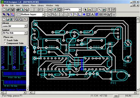
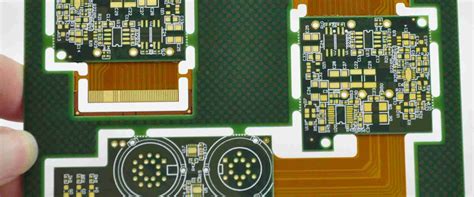
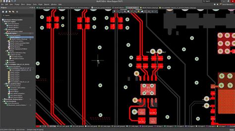
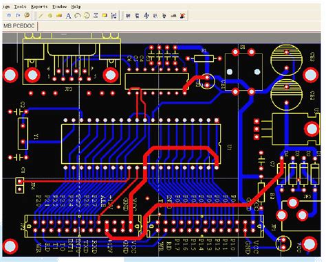
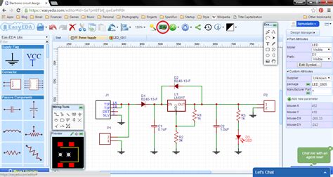
PCB design software is a specialized tool used by electronic engineers and designers to create, edit, and analyze PCB layouts. It allows users to design complex circuits, place components, route traces, and generate manufacturing files for PCB fabrication.

Key Features to Consider When Choosing PCB Design Software

Before diving into the comparison of different PCB design software, let’s discuss the essential features to look for:

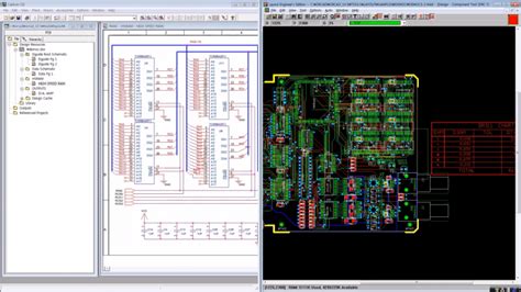
  1. Schematic Capture: The ability to create and edit schematic diagrams is a fundamental feature of any PCB design software. It should provide a user-friendly interface for placing components, drawing connections, and managing hierarchical designs.

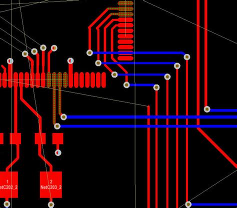
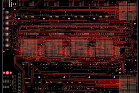
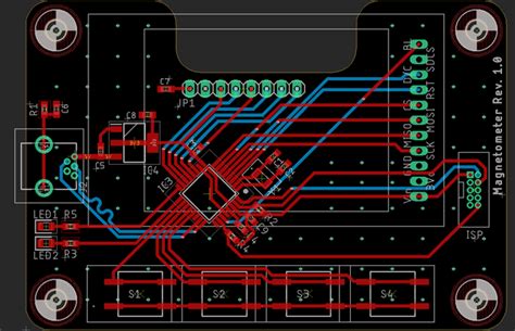
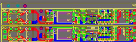
  2. PCB Layout: The software should offer powerful tools for PCB layout, including component placement, trace routing, and design rule checking (DRC). It should support various board sizes, layers, and manufacturing constraints.

  3. Library Management: A comprehensive component library is essential for efficient PCB design. The software should provide a vast library of pre-built components and allow users to create and manage custom libraries.

  4. 3D Visualization: The ability to visualize the PCB design in 3D helps in identifying potential issues and ensuring proper component placement. Look for software that offers realistic 3D rendering and mechanical integration.

  5. Collaboration and Version Control: If you work in a team environment, the software should support collaboration features such as version control, design sharing, and real-time updates.

  6. Output Generation: The software should be capable of generating accurate manufacturing files, including Gerber files, drill files, and assembly drawings, to ensure smooth communication with PCB fabrication and assembly services.

Top PCB Design Software Solutions

Now, let’s explore some of the best PCB design software solutions available in the market:
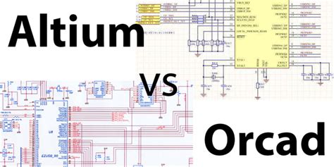
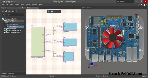
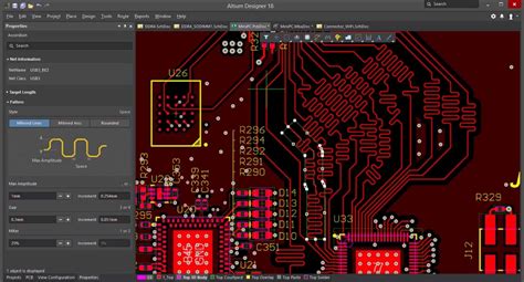
1. Altium Designer

Altium Designer is a powerful and comprehensive PCB design software that offers a wide range of features for both beginners and advanced users. It provides a seamless integration between schematic capture and PCB layout, allowing designers to efficiently create complex designs.

Feature Description
Schematic Capture Intuitive schematic editor with hierarchical design support and real-time design rule checking
PCB Layout Advanced layout tools, including interactive routing, 3D visualization, and rigid-flex PCB design
Library Management Extensive component library with access to online component databases and custom library creation
Simulation and Analysis Built-in signal integrity analysis, thermal simulation, and power distribution network analysis
Collaboration Altium 365 platform for real-time collaboration, version control, and design data management

Altium Designer is known for its robust feature set and industry-standard output generation. It is widely used by professional PCB designers and is suitable for complex, high-speed designs.

2. KiCad

KiCad is a free and open-source PCB design software that has gained popularity among hobbyists, students, and even professional designers. It offers a complete suite of tools for schematic capture, PCB layout, and 3D visualization.

Feature Description
Schematic Capture Eeschema schematic editor with hierarchical design support and integrated symbol library
PCB Layout Pcbnew layout editor with interactive routing, design rule checking, and 3D viewer
Library Management Extensive component library with support for custom symbol and footprint creation
Simulation and Analysis Integration with external simulation tools like SPICE and support for thermal analysis
Collaboration Version control integration with Git and design file format compatibility with other tools

KiCad’s strengths lie in its active community support, regular updates, and compatibility with various operating systems. It is an excellent choice for open-source enthusiasts and those on a tight budget.

3. Eagle

Eagle, now owned by Autodesk, is a popular PCB design software known for its ease of use and affordability. It offers a streamlined interface for schematic capture and PCB layout, making it suitable for beginners and small-scale projects.

Feature Description
Schematic Capture Schematic editor with real-time design rule checking and extensive component libraries
PCB Layout PCB layout editor with autorouter, design rule checking, and 3D visualization
Library Management Comprehensive component library with access to online libraries and custom library creation
Simulation and Analysis Integration with Autodesk Fusion 360 for mechanical design and simulation
Collaboration Cloud-based collaboration through Autodesk 360 platform and version control integration

Eagle’s strengths include its user-friendly interface, extensive component libraries, and integration with Autodesk’s ecosystem. It is a great choice for hobbyists, students, and small businesses.

4. OrCAD

OrCAD, developed by Cadence, is a professional-grade PCB design software known for its robustness and advanced features. It offers a comprehensive suite of tools for schematic capture, PCB layout, and simulation.

Feature Description
Schematic Capture OrCAD Capture schematic editor with hierarchical design support and real-time design rule checking
PCB Layout OrCAD PCB Designer with advanced routing, constraint management, and signal integrity analysis
Library Management Comprehensive component library with access to online component databases and custom library creation
Simulation and Analysis PSpice simulation for analog and mixed-signal designs and signal integrity analysis
Collaboration Cadence TeamShare for design collaboration, version control, and data management

OrCAD is widely used in the industry for complex and high-speed designs. It offers advanced features for signal integrity analysis, constraint management, and simulation.
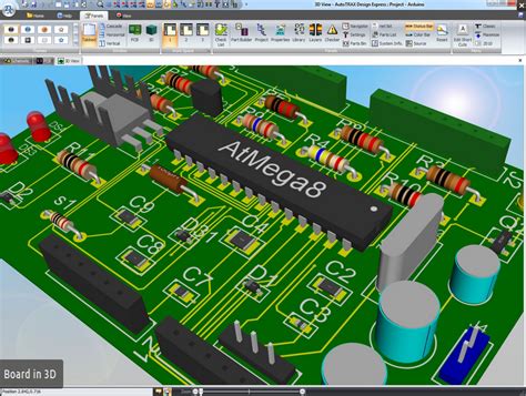
5. DipTrace

DipTrace is a user-friendly PCB design software that offers a balanced set of features for both beginners and experienced designers. It provides a smooth workflow from schematic capture to PCB layout and 3D visualization.

Feature Description
Schematic Capture Schematic editor with real-time design rule checking and component placement assistance
PCB Layout PCB layout editor with advanced routing, 3D visualization, and manufacturing output generation
Library Management Extensive component library with support for custom symbol and footprint creation
Simulation and Analysis Integration with external simulation tools and support for thermal analysis
Collaboration Version control integration and design file format compatibility with other tools

DipTrace’s strengths lie in its intuitive interface, affordable pricing, and active community support. It is a great choice for small to medium-sized projects and educational purposes.

Frequently Asked Questions (FAQ)

  1. Q: Which PCB design software is best for beginners?
    A: For beginners, KiCad and Eagle are excellent choices due to their user-friendly interfaces and extensive documentation. They offer a gentle learning curve and have active community support.

  2. Q: Is there a free PCB design software available?
    A: Yes, KiCad is a free and open-source PCB design software that offers a complete suite of tools for schematic capture, PCB layout, and 3D visualization. It is a great option for those on a tight budget.

  3. Q: Which PCB design software is widely used in the industry?
    A: Altium Designer and OrCAD are widely used in the industry for complex and high-speed designs. They offer advanced features for signal integrity analysis, constraint management, and simulation.

  4. Q: Can I import and export designs between different PCB design software?
    A: Most PCB design software support common file formats like Gerber, ODB++, and IPC-2581, which allow for design exchange between different tools. However, it’s always a good idea to check the compatibility and any potential limitations before migrating designs.

  5. Q: Do PCB design software offer simulation and analysis capabilities?
    A: Many PCB design software, such as Altium Designer and OrCAD, offer built-in simulation and analysis tools for signal integrity, thermal analysis, and power distribution network analysis. Some software also integrate with external simulation tools like SPICE for more advanced simulations.

Conclusion

Choosing the best PCB design software depends on your specific requirements, skill level, and budget. Altium Designer and OrCAD are industry-standard tools suitable for complex and high-speed designs, while KiCad and Eagle are great options for beginners and small-scale projects. DipTrace offers a balanced set of features at an affordable price point.

When selecting a PCB design software, consider factors such as ease of use, feature set, library management, simulation capabilities, and collaboration options. It’s also essential to evaluate the learning resources, community support, and compatibility with your existing design workflow.

Ultimately, the best PCB design software is the one that enables you to efficiently create high-quality PCB designs while meeting your project requirements and budget constraints. We hope this comprehensive guide has provided you with valuable insights to make an informed decision when choosing your PCB design software.

Which PCB design software is best?

What is PCB Design Software?

PCB design software is a specialized tool used by engineers and designers to create and layout printed circuit boards. These software packages offer a range of features and capabilities that streamline the PCB design process, from schematic capture to board layout and routing. By using PCB design software, designers can ensure that their PCBs are functionally correct, adhere to industry standards, and are optimized for manufacturing.

Key Features of PCB Design Software

When evaluating PCB design software, there are several key features to consider:

Schematic Capture

Schematic capture is the process of creating a graphical representation of the electronic circuit. A good PCB design software should offer an intuitive schematic editor with a comprehensive library of components and symbols. It should also support hierarchical design, allowing you to break down complex circuits into smaller, more manageable sub-circuits.

Board Layout and Routing

Once the schematic is complete, the next step is to lay out the components on the PCB and route the connections between them. The PCB design software should provide a powerful and flexible layout editor with features such as auto-placement, auto-routing, and design rule checking (DRC). It should also support multi-layer boards and provide tools for managing signal integrity and electromagnetic compatibility (EMC).

3D Visualization

Many modern PCB design software packages offer 3D visualization capabilities, allowing you to view your PCB design from various angles and check for potential mechanical interferences. This feature is particularly useful for designing complex boards with high component density or irregular shapes.

Simulation and Analysis

To ensure the reliability and performance of your PCB, it’s essential to perform simulations and analysis during the design phase. Some PCB design software includes built-in simulation tools for signal integrity, power integrity, and thermal analysis. These tools help identify potential issues early in the design process, reducing the risk of costly redesigns later on.

Manufacturing Output

Once your PCB design is complete, you’ll need to generate the necessary files for manufacturing. The PCB design software should be able to export industry-standard formats such as Gerber files, drill files, and bill of materials (BOM). It should also provide tools for generating assembly drawings and pick-and-place files.

PCB-design-software-b291b13be0ea11ee9e49201e88193817.jpeg” alt=”” class=”wp-image-136″ srcset=”https://pcb-copy.com/wp-content/uploads/2024/03/PCB-design-software-b291b13be0ea11ee9e49201e88193817.jpeg”>

Top PCB Design Software Options

Now that we’ve covered the key features to look for in PCB design software, let’s take a closer look at some of the top options available in the market.

1. Altium Designer

Altium Designer is a professional-grade PCB design software that offers a comprehensive set of features for schematic capture, board layout, and manufacturing output. It has a user-friendly interface and provides a seamless workflow from concept to production. Altium Designer also includes advanced features such as 3D visualization, signal integrity analysis, and automatic design rule checking.

Feature Description
Schematic Capture Intuitive schematic editor with a vast library of components and symbols
Board Layout Powerful layout editor with auto-placement, auto-routing, and multi-layer support
3D Visualization Realistic 3D rendering of the PCB for checking mechanical interferences
Simulation and Analysis Built-in tools for signal integrity, power integrity, and thermal analysis
Manufacturing Output Generates industry-standard output files for manufacturing

2. KiCad

KiCad is a free and open-source PCB design software that has gained popularity among hobbyists and small businesses. Despite being free, KiCad offers a robust set of features for schematic capture, board layout, and manufacturing output. It has an active community of users and developers who contribute to its development and provide support through forums and documentation.

Feature Description
Schematic Capture Schematic editor with a growing library of components and symbols
Board Layout Capable layout editor with auto-routing and design rule checking
3D Visualization Basic 3D rendering of the PCB for visual inspection
Simulation and Analysis Limited built-in simulation tools, but can export to third-party tools
Manufacturing Output Generates industry-standard output files for manufacturing

3. Eagle

Eagle is a popular PCB design software that is known for its ease of use and affordability. It offers a streamlined workflow for schematic capture, board layout, and manufacturing output. Eagle has a large community of users who contribute to its extensive library of components and design templates. While it may not have all the advanced features of more expensive software, Eagle is a solid choice for small to medium-sized projects.

Feature Description
Schematic Capture User-friendly schematic editor with a large library of components
Board Layout Intuitive layout editor with auto-routing and design rule checking
3D Visualization Basic 3D rendering of the PCB for visual inspection
Simulation and Analysis Limited built-in simulation tools
Manufacturing Output Generates industry-standard output files for manufacturing

4. OrCAD

OrCAD is a professional-grade PCB design software that is widely used in the electronics industry. It offers a comprehensive set of features for schematic capture, board layout, and simulation. OrCAD is known for its robustness and reliability, making it a popular choice for large-scale projects and complex designs. It also integrates well with other Cadence tools for a complete electronics design workflow.

Feature Description
Schematic Capture Powerful schematic editor with a vast library of components and symbols
Board Layout Advanced layout editor with auto-placement, auto-routing, and multi-layer support
3D Visualization Realistic 3D rendering of the PCB for checking mechanical interferences
Simulation and Analysis Comprehensive simulation tools for signal integrity, power integrity, and thermal analysis
Manufacturing Output Generates industry-standard output files for manufacturing

5. DipTrace

DipTrace is a user-friendly PCB design software that offers a complete solution for schematic capture, board layout, and manufacturing output. It has an intuitive interface and provides a smooth workflow for designing PCBs of various complexities. DipTrace also includes features such as 3D visualization, auto-routing, and design rule checking, making it a versatile choice for a wide range of projects.

Feature Description
Schematic Capture Easy-to-use schematic editor with a growing library of components
Board Layout Capable layout editor with auto-routing and design rule checking
3D Visualization Realistic 3D rendering of the PCB for visual inspection
Simulation and Analysis Basic simulation tools for signal integrity and EMC analysis
Manufacturing Output Generates industry-standard output files for manufacturing

Choosing the Right PCB Design Software

With so many PCB design software options available, it can be difficult to determine which one is the best fit for your needs. Here are some factors to consider when making your decision:

Project Complexity

The complexity of your PCB design project should be a key factor in choosing the right software. If you’re working on simple, single-layer boards, a basic software package like Eagle or KiCad may suffice. However, if you’re designing complex, multi-layer boards with high-speed signals, you may need the advanced features offered by Altium Designer or OrCAD.

Budget

PCB design software can vary greatly in price, from free options like KiCad to high-end packages like Altium Designer that can cost several thousand dollars. Consider your budget and the long-term cost of ownership when making your decision. Keep in mind that while free software may be appealing, it may lack the features and support you need for professional-grade projects.

User Experience

The user experience is another important factor to consider when choosing PCB design software. Look for software with an intuitive interface and a smooth workflow that allows you to focus on your design rather than struggling with the tools. Many software packages offer free trials or demos, so take advantage of these to get a feel for the user experience before making a purchase.

Community and Support

Having access to a strong community of users and reliable support can be invaluable when working with PCB design software. Look for software with an active user community, comprehensive documentation, and responsive technical support. This can help you quickly overcome any challenges you may face during the design process and ensure that you’re using the software effectively.

Integration with Other Tools

If you’re using other tools in your electronics design workflow, such as simulation software or CAD packages, consider how well the PCB design software integrates with these tools. Seamless integration can streamline your workflow and reduce the risk of errors when transferring data between different software packages.

Frequently Asked Questions (FAQ)

1. What is the best free PCB design software?

KiCad is widely considered to be the best free PCB design software available. It offers a comprehensive set of features for schematic capture, board layout, and manufacturing output, and has an active community of users and developers.

2. Is Eagle better than KiCad?

Both Eagle and KiCad are capable PCB design software packages, and the choice between them largely depends on your specific needs and preferences. Eagle is known for its ease of use and affordability, while KiCad is a free and open-source alternative with a growing feature set.

3. Can I use PCB design software on a Mac?

Yes, many PCB design software packages, including Altium Designer, KiCad, and Eagle, offer versions that are compatible with macOS. However, some software may have limited features or performance on macOS compared to their Windows counterparts.

4. How much does professional PCB design software cost?

The cost of professional PCB design software can vary widely, from a few hundred dollars to several thousand dollars. High-end packages like Altium Designer and OrCAD can cost upwards of $5,000 for a single license, while mid-range options like Eagle and DipTrace are more affordable, with prices ranging from $500 to $1,500.

5. Can I import designs from one PCB design software to another?

In most cases, yes. Many PCB design software packages support industry-standard file formats such as ODB++, IPC-2581, and Gerber, which allow you to transfer designs between different software tools. However, some software may have proprietary file formats that are not compatible with other packages, so it’s important to check the import and export capabilities of the software you’re considering.

Conclusion

Choosing the right PCB design software is a critical decision that can have a significant impact on the success of your electronics projects. By understanding the key features to look for and evaluating your specific needs and budget, you can select a software package that will help you efficiently design high-quality PCBs.

While there is no one-size-fits-all solution, the top PCB design software options discussed in this article – Altium Designer, KiCad, Eagle, OrCAD, and DipTrace – each offer a range of capabilities and benefits that can suit different project requirements and user preferences. Ultimately, the best PCB design software for you will depend on your level of experience, the complexity of your projects, and your long-term goals as an electronics designer.

Is Altium good for PCB design?

Introduction to PCB Design and Altium

Printed Circuit Board (PCB) design is a crucial aspect of electronic product development. It involves creating a layout of electronic components and copper traces on a non-conductive substrate to form a functional circuit. PCB design software plays a vital role in this process, enabling designers to create, simulate, and manufacture high-quality PCBs efficiently. Among the various PCB design software available in the market, Altium has gained significant popularity. In this article, we will explore the features and benefits of Altium and determine whether it is a good choice for PCB design.

What is Altium?

Altium is a comprehensive PCB design software that offers a wide range of features and tools for designing, simulating, and manufacturing electronic circuits. It is developed by Altium Limited, an Australian software company that specializes in electronic design automation (EDA) solutions. Altium provides a unified platform for schematic capture, PCB layout, 3D visualization, simulation, and documentation, making it a versatile tool for PCB designers.

Key Features of Altium for PCB Design

1. Schematic Capture

Altium offers a powerful schematic capture tool that allows designers to create, edit, and manage electronic schematics easily. It provides a wide range of schematic symbols and libraries, enabling designers to quickly create complex circuits. The schematic capture tool also supports hierarchical design, multi-sheet schematics, and intelligent pin swapping, making it efficient for designing large-scale projects.

2. PCB Layout

The PCB layout feature in Altium is highly advanced and user-friendly. It provides a comprehensive set of tools for placing components, routing traces, and defining board stackups. Altium’s interactive routing engine enables designers to route complex circuits efficiently while adhering to design rules and constraints. It also supports advanced features like length tuning, differential pair routing, and high-speed design techniques.

3. 3D Visualization

Altium offers a built-in 3D visualization tool that allows designers to view their PCB designs in a realistic 3D environment. This feature helps in identifying potential mechanical interferences, clearance issues, and component placement problems early in the design process. The 3D visualization also enables designers to generate photorealistic renderings of their PCBs for presentations and documentation.

4. Simulation and Analysis

Altium integrates powerful simulation and analysis tools that enable designers to validate their designs before manufacturing. It supports various types of simulations, including signal integrity analysis, power integrity analysis, and electromagnetic compatibility (EMC) analysis. These simulations help in identifying and resolving potential issues related to signal quality, power distribution, and electromagnetic interference.

5. Design Rule Checking (DRC)

Altium’s Design Rule Checking (DRC) feature ensures that the PCB design adheres to the specified design rules and constraints. It performs comprehensive checks for electrical and physical rules, such as clearance, width, spacing, and manufacturability. The DRC tool helps in identifying and resolving design rule violations, reducing the chances of manufacturing defects and improving the overall quality of the PCB.

6. Component Management

Altium provides a robust component management system that allows designers to create, organize, and manage their component libraries efficiently. It supports the creation of custom component footprints, 3D models, and parametric components. Altium also integrates with external component databases, enabling designers to access and import component information seamlessly.

7. Collaboration and Version Control

Altium offers collaboration and version control features that facilitate teamwork and project management. It supports real-time collaboration, allowing multiple designers to work on the same project simultaneously. The version control system tracks changes made to the design files, enabling designers to revert to previous versions if needed and maintain a complete history of the project.

Advantages of Using Altium for PCB Design

1. Comprehensive Feature Set

Altium provides a comprehensive set of features and tools that cover all aspects of PCB design, from schematic capture to manufacturing. It offers a unified platform that integrates schematic design, PCB layout, simulation, and documentation, eliminating the need for multiple software tools and ensuring a seamless design flow.

2. User-Friendly Interface

Altium has a user-friendly interface that is intuitive and easy to navigate. It provides a customizable workspace, context-sensitive menus, and keyboard shortcuts, enabling designers to work efficiently and productively. The interface also supports multi-monitor setups, allowing designers to spread their work across multiple screens for better visualization and organization.

3. Extensive Libraries and Templates

Altium comes with an extensive collection of libraries and templates that accelerate the design process. It includes a wide range of schematic symbols, PCB footprints, and 3D models for common electronic components. Altium also provides pre-defined templates for various PCB design standards and applications, saving designers time and effort in setting up their projects.

4. Powerful Automation Tools

Altium offers powerful automation tools that streamline repetitive tasks and improve design efficiency. It supports scripting and automation through its built-in scripting language, enabling designers to automate complex design tasks and create custom utilities. Altium also provides a design reuse feature that allows designers to save and reuse commonly used design elements, reducing design time and ensuring consistency across projects.

5. Robust Simulation and Analysis Capabilities

Altium’s integrated simulation and analysis tools enable designers to validate their designs and identify potential issues early in the design process. It supports various types of simulations, including signal integrity analysis, power integrity analysis, and EMC analysis. These simulations help in optimizing the design for performance, reliability, and manufacturability, reducing the risk of costly redesigns and manufacturing defects.

6. Collaborative Design Environment

Altium supports collaboration and teamwork through its real-time collaboration and version control features. Multiple designers can work on the same project simultaneously, with changes synchronized in real-time. The version control system tracks all changes made to the design files, allowing designers to revert to previous versions and maintain a complete history of the project. This collaborative environment improves communication, coordination, and efficiency among team members.

7. Manufacturing Output and Documentation

Altium provides comprehensive manufacturing output and documentation features. It supports the generation of various manufacturing files, such as Gerber files, drill files, and pick-and-place files, ensuring accurate and reliable communication with PCB fabrication and assembly vendors. Altium also generates detailed documentation, including schematic diagrams, PCB layouts, bill of materials (BOM), and assembly drawings, facilitating the manufacturing and assembly process.

Comparison with Other PCB Design Software

To determine whether Altium is a good choice for PCB design, it is essential to compare it with other popular PCB design software available in the market. The following table provides a comparison of Altium with two other widely used PCB design software: KiCad and Eagle.

Feature Altium KiCad Eagle
Schematic Capture Advanced Basic Basic
PCB Layout Advanced Intermediate Intermediate
3D Visualization Built-in Built-in Add-on
Simulation and Analysis Integrated Limited Limited
Design Rule Checking Comprehensive Basic Basic
Component Management Advanced Basic Intermediate
Collaboration Real-time Limited Limited
User Interface User-friendly Moderate User-friendly
Price High Free Moderate

As shown in the comparison table, Altium stands out in terms of its advanced features, comprehensive capabilities, and user-friendly interface. However, it comes with a higher price tag compared to KiCad and Eagle. KiCad is a free and open-source PCB design software that offers basic to intermediate features, while Eagle is a moderately priced software with intermediate capabilities.

Frequently Asked Questions (FAQ)

1. Is Altium suitable for beginners in PCB design?

While Altium is a powerful and feature-rich software, it may have a steeper learning curve compared to simpler PCB design tools. However, Altium provides extensive documentation, tutorials, and online resources to help beginners get started. With dedication and practice, beginners can leverage Altium’s advanced features and become proficient in PCB design.

2. Can Altium handle complex and high-speed PCB designs?

Yes, Altium is well-suited for designing complex and high-speed PCBs. It offers advanced features like length tuning, differential pair routing, and impedance control, which are essential for high-speed designs. Altium’s simulation and analysis tools also help in optimizing signal integrity and power distribution for complex circuits.

3. Does Altium support multi-board designs?

Yes, Altium supports multi-board designs through its multi-board assembly feature. It allows designers to create and manage multiple PCBs within a single project, enabling seamless connectivity and synchronization between the boards. This feature is particularly useful for designing complex systems with multiple interconnected PCBs.

4. Can Altium import and export design files from other PCB design software?

Altium supports various file formats for importing and exporting design files. It can import schematic and PCB designs from other popular PCB design software, such as Eagle, KiCad, and OrCAD. Altium can also export design files in standard formats like Gerber, ODB++, and IPC-2581, ensuring compatibility with different PCB fabrication and assembly vendors.

5. Is Altium cloud-based or locally installed?

Altium is primarily a locally installed software that runs on Windows operating systems. However, Altium also offers cloud-based services like Altium 365, which provides online storage, collaboration, and version control features. Designers can choose to use Altium as a standalone locally installed software or leverage the cloud-based services for enhanced collaboration and accessibility.

Conclusion

In conclusion, Altium is a powerful and comprehensive PCB design software that offers a wide range of features and benefits for designing high-quality electronic circuits. Its advanced schematic capture, PCB layout, simulation, and documentation capabilities make it a versatile tool for both beginners and experienced PCB designers. Altium’s user-friendly interface, extensive libraries, and automation tools streamline the design process and improve productivity.

Compared to other PCB design software like KiCad and Eagle, Altium stands out in terms of its advanced features and comprehensive capabilities. However, it comes with a higher price tag, which may be a consideration for some users.

Overall, if you are looking for a feature-rich and powerful PCB design software that can handle complex designs and provide a collaborative design environment, Altium is definitely a good choice. Its extensive features, user-friendly interface, and robust simulation and analysis tools make it a valuable asset for any PCB design project.

What is the full form of PCB in project?

Introduction to PCB

PCB stands for Printed Circuit Board. It is a fundamental component in modern electronic devices and projects. A PCB is a flat board made of insulating material, such as fiberglass or plastic, with conductive copper traces printed on its surface. These traces connect various electronic components, such as resistors, capacitors, and integrated circuits (ICs), to form a complete electrical circuit.

History of PCBs

The concept of printed circuits dates back to the early 20th century. In 1903, Albert Hanson, a German inventor, filed a patent for a method of creating conductive patterns on an insulating substrate. However, it wasn’t until the 1940s that PCBs began to gain widespread use in electronic devices.

During World War II, the United States military heavily relied on PCBs for their electronic equipment, such as radios and radar systems. The use of PCBs allowed for more compact and reliable electronic devices, which were crucial for military applications.

After the war, PCBs became more widely adopted in consumer electronics, such as televisions and radios. As electronic devices became more complex and miniaturized, the demand for PCBs grew exponentially.

Manufacturing Process

The manufacturing process of PCBs involves several steps:

  1. Design: The first step is to design the PCB layout using specialized software, such as Eagle or KiCad. The design includes the placement of components, routing of traces, and creation of ground planes.

  2. Printing: Once the design is finalized, the PCB layout is printed onto a transparent film or directly onto the copper-clad board using a photoplotter.

  3. Etching: The printed board is then placed in an etching solution, which removes the unwanted copper from the board, leaving only the desired traces and pads.

  4. Drilling: Holes are drilled into the board for through-hole components and vias, which connect traces on different layers of the board.

  5. Plating: The drilled holes are plated with copper to ensure electrical conductivity between layers.

  6. Solder Mask: A solder mask is applied to the board to protect the copper traces from oxidation and to prevent accidental short circuits during soldering.

  7. Silkscreen: A silkscreen layer is added to the board, which includes text and symbols to indicate component placement and other important information.

  8. Assembly: Finally, the electronic components are soldered onto the board, either manually or using automated pick-and-place machines.

Types of PCBs

There are several types of PCBs, each with its own unique characteristics and applications.

Single-Layer PCBs

Single-layer PCBs, also known as single-sided PCBs, have conductive traces on only one side of the board. They are the simplest and most cost-effective type of PCB, making them ideal for low-complexity projects and prototypes.

Double-Layer PCBs

Double-layer PCBs, also known as double-sided PCBs, have conductive traces on both sides of the board. They offer more routing options and higher component density compared to single-layer PCBs. Double-layer PCBs are commonly used in more complex projects, such as consumer electronics and industrial control systems.

Multi-Layer PCBs

Multi-layer PCBs have three or more conductive layers, with insulating layers sandwiched between them. They offer the highest component density and routing options, making them suitable for highly complex projects, such as smartphones, computers, and aerospace applications.

Type Layers Complexity Cost Applications
Single-Layer 1 Low Low Simple projects, prototypes
Double-Layer 2 Medium Medium Consumer electronics, control systems
Multi-Layer 3+ High High Smartphones, computers, aerospace

Flexible PCBs

Flexible PCBs, also known as flex circuits, are made from flexible materials, such as polyimide or PEEK. They can bend and twist without breaking, making them ideal for applications that require movement or tight spaces, such as wearable devices and automotive electronics.

Rigid-Flex PCBs

Rigid-flex PCBs combine the benefits of both rigid and flexible PCBs. They consist of rigid PCB sections connected by flexible PCB sections, allowing for three-dimensional assembly and improved reliability in high-stress applications, such as military and aerospace electronics.

PCB design Considerations

When designing a PCB, there are several important factors to consider to ensure optimal performance and reliability.

Component Placement

Proper component placement is crucial for several reasons:

  1. Signal Integrity: Components should be placed in a way that minimizes the length of critical signal traces, reducing the risk of signal degradation and electromagnetic interference (EMI).

  2. Thermal Management: Heat-generating components, such as power regulators and processors, should be placed in a way that allows for adequate cooling, either through natural convection or the use of heatsinks and fans.

  3. Mechanical Constraints: Components should be placed in a way that allows for easy assembly and maintenance, while also considering the mechanical constraints of the enclosure or housing.

Trace Routing

Trace routing is the process of creating the conductive paths that connect components on the PCB. Proper trace routing is essential for ensuring signal integrity and minimizing EMI.

Some key considerations for trace routing include:

  1. Trace Width: The width of a trace determines its current-carrying capacity and resistance. Wider traces can carry more current and have lower resistance, but they also take up more space on the board.

  2. Trace Spacing: The spacing between traces determines the risk of crosstalk and EMI. Traces should be spaced far enough apart to minimize these risks, while also considering the manufacturing capabilities of the PCB fabricator.

  3. Trace Length: The length of a trace determines its resistance and the risk of signal degradation. Critical signal traces should be kept as short as possible to minimize these risks.

Ground Planes

Ground planes are large areas of copper on the PCB that provide a low-impedance return path for electrical currents. They are essential for minimizing EMI and ensuring signal integrity.

When designing ground planes, it’s important to consider the following:

  1. Plane Placement: Ground planes should be placed on layers adjacent to signal layers to provide a low-impedance return path for currents.

  2. Plane Stitching: Ground planes on different layers should be connected together using vias, a process known as stitching, to ensure a continuous low-impedance return path.

  3. Plane Splits: In some cases, it may be necessary to split a ground plane into separate sections to isolate different parts of the circuit. This can be done using a technique called slotting, which involves creating a narrow gap in the ground plane.

Electromagnetic Compatibility (EMC)

EMC refers to the ability of an electronic device to function properly in its electromagnetic environment without causing interference to other devices. PCBs play a critical role in ensuring EMC, as they can be a source of EMI if not designed properly.

Some key considerations for EMC in PCB design include:

  1. Shielding: Sensitive components and traces can be shielded using metal enclosures or conductive coatings to reduce the risk of EMI.

  2. Filtering: Power supply lines and other noise-sensitive traces can be filtered using capacitors and ferrite beads to reduce the risk of EMI.

  3. Grounding: Proper grounding techniques, such as the use of ground planes and stitching, can help minimize EMI and ensure signal integrity.

PCB Assembly

Once the PCB design is finalized and the board is manufactured, the next step is to assemble the components onto the board. There are two main methods of PCB assembly: through-hole and surface mount.

Through-Hole Assembly

Through-hole assembly involves inserting component leads through holes drilled in the PCB and soldering them to pads on the opposite side of the board. This method is well-suited for larger components and provides a strong mechanical connection, but it requires more manual labor and takes up more space on the board compared to surface mount assembly.

Surface Mount Assembly

Surface mount assembly involves soldering components directly onto pads on the surface of the PCB. This method allows for higher component density and faster assembly compared to through-hole, but it requires more precise manufacturing techniques and specialized equipment.

Assembly Method Component Size Mechanical Strength Assembly Speed Component Density
Through-Hole Large High Slow Low
Surface Mount Small Low Fast High

Soldering Techniques

Soldering is the process of joining two metal surfaces using a molten metal alloy called solder. There are several soldering techniques used in PCB assembly, including:

  1. Hand Soldering: This method involves manually applying solder to components and pads using a soldering iron. It is well-suited for small-scale assembly and repairs, but it is time-consuming and requires a skilled operator.

  2. Wave Soldering: This method involves passing the PCB over a wave of molten solder, which selectively solders components to the board. It is well-suited for through-hole assembly and provides a fast and efficient way to solder multiple components at once.

  3. Reflow Soldering: This method involves applying solder paste to the PCB pads and placing components onto the paste. The board is then heated in a reflow oven, which melts the solder and secures the components to the board. It is well-suited for surface mount assembly and provides a fast and efficient way to solder multiple components at once.

PCB Testing and Inspection

After assembly, PCBs must be thoroughly tested and inspected to ensure they meet the required specifications and performance criteria. There are several methods of PCB testing and inspection, including:

Visual Inspection

Visual inspection involves examining the PCB for defects such as solder bridges, cold solder joints, and component misalignment. This can be done manually using a microscope or automated using machine vision systems.

Automated Optical Inspection (AOI)

AOI uses cameras and image processing algorithms to automatically detect defects on the PCB. It is faster and more accurate than manual visual inspection and can detect defects that are difficult to see with the naked eye.

In-Circuit Testing (ICT)

ICT involves using a bed-of-nails fixture to make electrical contact with specific points on the PCB and measuring the electrical characteristics of the circuit. This allows for detailed testing of individual components and connections, but it requires a custom fixture for each PCB design.

Functional Testing

Functional testing involves applying power to the PCB and testing its functionality under real-world operating conditions. This can be done using specialized test equipment or by integrating the PCB into the final product and testing it as part of the overall system.

Testing Method Defects Detected Speed Accuracy Cost
Visual Inspection Solder bridges, cold joints Slow Low Low
Automated Optical Inspection Solder defects, component placement Fast High Medium
In-Circuit Testing Component and connection faults Medium High High
Functional Testing Overall system functionality Slow High Medium

Conclusion

PCBs are an essential component in modern electronic devices and projects. They provide a reliable and efficient way to interconnect electronic components and form complete electrical circuits. Understanding the different types of PCBs, design considerations, assembly methods, and testing techniques is crucial for anyone involved in electronic product development.

As electronic devices continue to become more complex and miniaturized, the demand for high-quality PCBs will only continue to grow. By staying up-to-date with the latest PCB technologies and best practices, engineers and designers can create innovative and reliable electronic products that meet the needs of today’s rapidly evolving market.

FAQ

  1. What are the advantages of using PCBs in electronic projects?
  2. PCBs offer several advantages, including:

    • Compact and efficient packaging of electronic components
    • Reliable and consistent electrical connections
    • Improved signal integrity and reduced electromagnetic interference
    • Simplified assembly and manufacturing processes
    • Reduced overall system cost and improved reliability
  3. What software is used for PCB design?

  4. There are several software options available for PCB design, including:

    • Autodesk Eagle
    • KiCad
    • Altium Designer
    • Cadence OrCAD
    • Mentor Graphics PADS
  5. What are the different types of PCB materials?

  6. The most common PCB materials include:

    • FR-4: A composite material made of fiberglass and epoxy resin, widely used for its good mechanical and electrical properties
    • Polyimide: A flexible material used for flex circuits and high-temperature applications
    • Ceramic: Used for high-frequency and high-power applications due to its excellent thermal and dielectric properties
    • Aluminum: Used for heat dissipation in power electronics applications
  7. What is the difference between through-hole and surface mount assembly?

  8. Through-hole assembly involves inserting component leads through holes drilled in the PCB and soldering them to pads on the opposite side of the board. It offers strong mechanical connections but requires more manual labor and takes up more space.
  9. Surface mount assembly involves soldering components directly onto pads on the surface of the PCB. It allows for higher component density and faster assembly but requires more precise manufacturing techniques and specialized equipment.

  10. What are the key considerations for PCB testing and inspection?

  11. The key considerations for PCB testing and inspection include:
    • Detecting manufacturing defects such as solder bridges, cold solder joints, and component misalignment
    • Verifying the electrical characteristics of individual components and connections
    • Ensuring the overall functionality and performance of the PCB under real-world operating conditions
    • Choosing the appropriate testing methods based on the complexity and requirements of the PCB design
    • Balancing the cost, speed, and accuracy of different testing methods to optimize the overall manufacturing process.

What does a PCB stand for?

The History of Printed Circuit Boards

The concept of printed circuit boards can be traced back to the early 20th century. In 1903, Albert Hanson, a German inventor, filed a patent for a method of creating conductive patterns on an insulating material. However, it wasn’t until the 1940s that printed circuit boards began to gain widespread use in the electronics industry.

During World War II, the demand for compact and reliable electronic equipment increased significantly. In 1943, Paul Eisler, an Austrian engineer, developed a process for printing conductive ink onto a non-conductive substrate, which became the foundation for modern PCB manufacturing.

In the 1950s, the U.S. military adopted printed circuit boards for use in their electronic equipment, which further accelerated the development and adoption of PCB technology. By the 1960s, PCBs had become the standard method for assembling electronic circuits in both military and consumer applications.

The Manufacturing Process of PCBs

The manufacturing process of printed circuit boards involves several steps, each of which is critical to ensuring the quality and reliability of the final product. The main steps in PCB manufacturing are as follows:

  1. Design: The first step in creating a PCB is to design the circuit using specialized software, such as Eagle or KiCad. The design includes the placement of components, routing of conductive traces, and the creation of solder masks and silkscreen layers.

  2. Printing: Once the design is complete, the PCB layout is printed onto a transparent film or photomask. This film is used to transfer the circuit pattern onto the copper-clad board during the etching process.

  3. Etching: The copper-clad board is coated with a light-sensitive resist material and then exposed to UV light through the photomask. The areas of the resist that are exposed to light harden, while the unexposed areas remain soluble. The board is then placed in an etching solution, which removes the unprotected copper, leaving behind the desired conductive traces.

  4. Drilling: After etching, holes are drilled into the board to accommodate through-hole components and to create vias, which are used to connect traces on different layers of the board.

  5. Plating: The drilled holes are then plated with copper to ensure a reliable electrical connection between layers. Additional plating, such as tin-lead or gold, may be applied to improve solderability and prevent oxidation.

  6. Solder Mask and Silkscreen: A solder mask, typically green in color, is applied to the board to protect the copper traces from accidental short-circuits during soldering. A silkscreen layer, which contains text and symbols, is then added to help identify components and provide assembly instructions.

  7. Surface Mount Assembly: Surface mount components are placed onto the board using a pick-and-place machine, which uses computer vision to accurately position the components on the designated pads. The board is then run through a reflow oven, which melts the solder paste and permanently attaches the components to the board.

  8. Through-Hole Assembly: For through-hole components, the leads are inserted into the drilled holes, and the board is then sent through a wave soldering machine, which applies molten solder to the underside of the board, creating a connection between the component leads and the copper traces.

  9. Inspection and Testing: After assembly, the PCB undergoes various inspections and tests to ensure proper functionality and adherence to quality standards. This may include visual inspections, automated optical inspections (AOI), X-ray inspections, and electrical testing.

Types of Printed Circuit Boards

There are several types of printed circuit boards, each with its own unique characteristics and applications. The most common types of PCBs are:

  1. Single-Sided PCBs: These boards have conductive traces on only one side of the insulating substrate. Single-sided PCBs are the simplest and most cost-effective option, making them suitable for low-complexity circuits and prototypes.

  2. Double-Sided PCBs: As the name suggests, double-sided PCBs have conductive traces on both sides of the insulating substrate. The two sides are connected using through-hole vias, allowing for more complex circuits and higher component density compared to single-sided boards.

  3. Multi-Layer PCBs: These boards consist of multiple layers of insulating material and conductive traces, sandwiched together to form a single board. Multi-layer PCBs can have anywhere from four to over thirty layers, allowing for extremely complex circuits and high component density. They are commonly used in advanced electronic devices, such as smartphones, computers, and medical equipment.

  4. Flexible PCBs: Flexible PCBs are made using a flexible insulating material, such as polyimide, which allows the board to bend and conform to various shapes. They are often used in applications where space is limited or where the board needs to fit into a specific form factor, such as in wearable devices or automotive electronics.

  5. Rigid-Flex PCBs: Rigid-flex PCBs combine the benefits of both rigid and flexible boards. They consist of rigid sections, which provide structural support and house most of the components, and flexible sections, which allow the board to bend and fold as needed. Rigid-flex PCBs are commonly used in aerospace, military, and medical applications.

Advantages of Using Printed Circuit Boards

Printed circuit boards offer numerous advantages over other methods of assembling electronic circuits, such as point-to-point wiring or wire-wrap. Some of the key benefits of using PCBs include:

  1. Consistency and Reliability: PCBs are manufactured using automated processes, which ensures a high degree of consistency and reliability between boards. This reduces the risk of errors and improves the overall quality of the final product.

  2. Compact Size: By using PCBs, electronic circuits can be made much smaller and more compact than with other assembly methods. This is particularly important in modern electronic devices, where space is often at a premium.

  3. Reduced Assembly Time: PCBs allow for automated assembly processes, such as pick-and-place and reflow soldering, which significantly reduces the time required to assemble a complete circuit. This can lead to faster production times and lower manufacturing costs.

  4. Improved Signal Integrity: The precise layout and routing of conductive traces on a PCB help to minimize signal interference and crosstalk, which is essential for high-speed and high-frequency applications.

  5. Easier Maintenance and Repair: PCBs make it easier to identify and replace faulty components, as each component has a designated location on the board. This can simplify maintenance and repair tasks, reducing downtime and associated costs.

Applications of Printed Circuit Boards

Printed circuit boards are used in virtually every electronic device, from simple consumer gadgets to complex industrial equipment. Some of the most common applications of PCBs include:

  1. Consumer Electronics: PCBs are found in a wide range of consumer devices, such as smartphones, tablets, laptops, televisions, gaming consoles, and home appliances.

  2. Automotive Electronics: Modern vehicles rely heavily on electronic systems for various functions, such as engine management, infotainment, and advanced driver assistance systems (ADAS). PCBs are essential components in these systems, providing reliable and compact solutions for automotive applications.

  3. Medical Devices: PCBs are used in numerous medical devices, including patient monitors, imaging equipment, and implantable devices such as pacemakers and defibrillators. In these applications, PCBs must meet stringent quality and reliability standards to ensure patient safety.

  4. Industrial Equipment: PCBs are used in a variety of industrial applications, such as process control systems, automation equipment, and power electronics. In these environments, PCBs must be designed to withstand harsh conditions, such as extreme temperatures, vibration, and exposure to chemicals.

  5. Aerospace and Defense: PCBs are critical components in aerospace and defense applications, where reliability and performance are paramount. Examples include avionics systems, radar equipment, and satellite communications hardware.

PCB design Considerations

Designing a printed circuit board involves several key considerations to ensure optimal performance, reliability, and manufacturability. Some of the most important aspects of PCB design include:

  1. Component Placement: The placement of components on a PCB can have a significant impact on signal integrity, thermal management, and manufacturability. Designers must consider factors such as component size, pin spacing, and heat dissipation when determining the optimal placement.

  2. Trace Routing: The routing of conductive traces on a PCB is critical for ensuring proper signal integrity and minimizing interference. Designers must consider factors such as trace width, spacing, and impedance when routing traces, particularly for high-speed or high-frequency signals.

  3. Grounding and Shielding: Proper grounding and shielding techniques are essential for minimizing electromagnetic interference (EMI) and ensuring stable operation. This may involve the use of ground planes, shielding layers, and careful placement of sensitive components.

  4. Thermal Management: Managing heat dissipation is crucial for ensuring the long-term reliability of a PCB and its components. Designers must consider factors such as component power ratings, ambient temperatures, and available cooling methods when designing for thermal management.

  5. Manufacturing Constraints: PCB designers must also consider the limitations and capabilities of the manufacturing process when creating their designs. This includes factors such as minimum trace widths, hole sizes, and clearances, as well as the availability of specific materials or surface finishes.

Frequently Asked Questions (FAQ)

  1. What is the difference between a PCB and a printed wiring board (PWB)?
  2. A printed wiring board (PWB) is a more general term that includes both printed circuit boards (PCBs) and other types of boards that use conductive traces for interconnections. In practice, however, the terms PCB and PWB are often used interchangeably.

  3. What materials are used to make PCBs?

  4. The most common base material for PCBs is FR-4, which is a composite material made from woven fiberglass and epoxy resin. Other materials, such as polyimide, ceramic, and metal-core substrates, may be used for specific applications or environments.

  5. How are PCBs tested for quality and reliability?

  6. PCBs undergo various tests to ensure quality and reliability, including visual inspections, automated optical inspections (AOI), X-ray inspections, and electrical tests such as continuity, insulation resistance, and high-potential (hipot) testing. Environmental stress tests, such as thermal cycling and humidity exposure, may also be performed to validate the board’s performance under specific conditions.

  7. What is the typical turnaround time for PCB manufacturing?

  8. The turnaround time for PCB manufacturing varies depending on factors such as board complexity, layer count, and the manufacturer’s capacity. Simple, single-sided boards may be produced in as little as 24 hours, while complex, multi-layer boards may take several weeks. Most PCB manufacturers offer standard lead times of 5-15 business days for typical orders.

  9. How can I ensure my PCB design is ready for manufacturing?

  10. To ensure your PCB design is ready for manufacturing, you should work closely with your chosen PCB manufacturer and adhere to their design guidelines. This includes factors such as minimum trace widths, hole sizes, and clearances, as well as the use of appropriate design file formats (e.g., Gerber, ODB++). Many PCB manufacturers offer design review services to help identify and address potential issues before production begins.
PCB Type Layers Typical Applications
Single-Sided 1 Simple circuits, prototypes, low-cost products
Double-Sided 2 Moderately complex circuits, consumer electronics
Multi-Layer 4+ Complex circuits, high-density designs, advanced electronics
Flexible 1+ Wearables, automotive, aerospace, medical devices
Rigid-Flex 2+ Aerospace, military, medical devices, high-reliability applications

In conclusion, printed circuit boards (PCBs) are essential components in modern electronics, providing a reliable and efficient means of interconnecting electronic components. From their early beginnings in the 20th century to their widespread use today, PCBs have enabled the development of increasingly complex and compact electronic devices across a wide range of industries and applications.

As technology continues to advance, the design and manufacturing of PCBs will play a crucial role in shaping the future of electronics, enabling new innovations and pushing the boundaries of what is possible.

How do you reproduce PCB?

Keywords

Understanding the PCB

Before attempting to reproduce a PCB, it is essential to understand its structure and components. A PCB typically consists of the following layers:

  1. Substrate: The base material, usually made of fiberglass or other insulating materials.
  2. Copper layers: Thin sheets of copper laminated onto the substrate, forming the conductive pathways.
  3. Solder mask: A protective layer applied over the copper, leaving only the necessary exposed areas for soldering.
  4. Silkscreen: A printed layer that adds text, symbols, and logos for easier identification and assembly.
Layer Description
Substrate Insulating base material
Copper Conductive pathways
Solder Mask Protective layer over copper
Silkscreen Printed text and symbols

PCB Components

PCBs also contain various electronic components, such as:

  • Resistors
  • Capacitors
  • Inductors
  • Diodes
  • Transistors
  • Integrated Circuits (ICs)

These components are soldered onto the exposed copper areas of the PCB, allowing them to interconnect and form a functional electronic circuit.

PCB Reproduction Methods

There are several methods for reproducing PCBs, each with its own advantages and limitations. The choice of method depends on factors such as the complexity of the board, available resources, and the desired level of accuracy.

1. Manual Tracing

Manual tracing involves carefully examining the original PCB and manually recreating the copper traces and component layouts on a new board. This method is suitable for simple PCBs with few layers and components.

Steps for Manual Tracing

  1. Clean the original PCB to remove any dirt or debris.
  2. Use a magnifying glass or microscope to closely inspect the copper traces and component placements.
  3. Sketch the PCB layout on paper, accurately representing the traces and components.
  4. Transfer the sketch onto a new PCB substrate using a permanent marker or etch-resistant pen.
  5. Etch away the unwanted copper areas using a chemical etching solution, leaving only the desired traces.
  6. Drill holes for through-hole components and vias.
  7. Apply solder mask and silkscreen layers if necessary.
  8. Solder the components onto the new PCB.

2. Image-Based Reproduction

Image-based reproduction involves capturing high-resolution images of the original PCB and using image processing software to extract the copper traces and component layouts. This method is more accurate than manual tracing and can handle more complex PCBs.

Steps for Image-Based Reproduction

  1. Clean the original PCB and ensure it is free from glare and reflections.
  2. Capture high-resolution images of both sides of the PCB using a digital camera or scanner.
  3. Use image processing software to enhance the contrast and clarity of the captured images.
  4. Manually or automatically trace the copper traces and component outlines using the software.
  5. Convert the traced data into a suitable PCB design format, such as Gerber or ODB++.
  6. Manufacture the new PCB using the generated design files.

3. X-Ray Imaging

For multi-layer PCBs or boards with hidden traces, X-ray imaging can be used to capture the internal structure of the PCB. This method provides a detailed view of the copper layers and vias, allowing for accurate reproduction.

Steps for X-Ray Imaging

  1. Place the original PCB in an X-ray machine.
  2. Capture X-ray images of the PCB from various angles to cover all layers and features.
  3. Process the captured images using specialized software to extract the layer information and generate a 3D model of the PCB.
  4. Use the generated 3D model to create the necessary design files for manufacturing the new PCB.

Comparison of Reproduction Methods

Method Complexity Accuracy Cost
Manual Tracing Low Low Low
Image-Based Medium Medium Medium
X-Ray Imaging High High High

PCB Reverse Engineering

In some cases, reproducing a PCB may require reverse engineering the original design. This involves analyzing the PCB to understand its schematic, components, and functionality. Reverse engineering is particularly useful when the original design files or documentation are not available.

Steps for PCB Reverse Engineering

  1. Identify the components on the PCB and create a bill of materials (BOM).
  2. Trace the connections between components and create a schematic diagram.
  3. Analyze the schematic to understand the circuit’s functionality and identify any sub-circuits or modules.
  4. Create a new PCB layout based on the reverse-engineered schematic, optimizing the design if necessary.
  5. Verify the new design by comparing it with the original PCB and conducting functional tests.

PCB Reproduction Services

For those who lack the necessary skills, equipment, or time to reproduce PCBs themselves, there are professional PCB reproduction services available. These services typically offer a range of options, from simple PCB duplication to full reverse engineering and redesign.

Advantages of Using PCB Reproduction Services

  • Expertise: Professional services have experienced engineers and technicians who can handle complex PCBs and ensure high-quality results.
  • Equipment: Reproduction services have access to advanced equipment, such as X-ray machines and high-resolution scanners, which may not be available to individuals.
  • Time-saving: Outsourcing the PCB reproduction process can save significant time and effort, allowing you to focus on other aspects of your project.

Choosing a PCB Reproduction Service

When selecting a PCB reproduction service, consider the following factors:

  1. Experience: Look for a service with a proven track record of successfully reproducing PCBs similar to yours.
  2. Capabilities: Ensure that the service has the necessary equipment and expertise to handle your specific PCB reproduction needs.
  3. Turnaround time: Consider the service’s turnaround time and whether it meets your project deadlines.
  4. Cost: Compare the costs of different services and choose one that offers the best value for your budget.

Frequently Asked Questions (FAQ)

  1. Q: Can any PCB be reproduced?
    A: In most cases, yes. However, the complexity of the PCB and the availability of the original design files can affect the feasibility and accuracy of the reproduction process.

  2. Q: How long does it take to reproduce a PCB?
    A: The time required to reproduce a PCB depends on the chosen method and the complexity of the board. Simple PCBs can be reproduced in a matter of hours, while complex boards may take several days or weeks.

  3. Q: Is it legal to reproduce PCBs?
    A: Reproducing PCBs for personal use or repair purposes is generally legal. However, reproducing and selling PCBs without the original designer’s permission may infringe on intellectual property rights.

  4. Q: What are the costs involved in PCB reproduction?
    A: The costs of PCB reproduction vary depending on the method used, the complexity of the board, and the required materials. Professional reproduction services typically charge based on the board’s size, layer count, and the level of reverse engineering required.

  5. Q: Can I reproduce a PCB with missing components?
    A: Yes, it is possible to reproduce a PCB even if some components are missing. However, you will need to identify and source the missing components before assembling the reproduced board.

Conclusion

PCB reproduction is a valuable process for creating identical copies of existing PCBs, whether for replacement, backup, or mass production purposes. By understanding the structure and components of PCBs, and employing the appropriate reproduction methods, you can successfully replicate PCBs with varying levels of complexity. When in doubt, professional PCB reproduction services can provide the expertise and resources necessary to ensure high-quality results.

Can a PCB be copied?

Introduction to PCB Duplication

Printed Circuit Boards (PCBs) are essential components in modern electronic devices, ranging from smartphones and computers to industrial equipment and medical devices. As technology advances and the demand for electronic products grows, the question arises: Can a PCB be copied? In this article, we will explore the concept of PCB duplication, its techniques, advantages, and challenges.

What is PCB Duplication?

PCB duplication is the process of creating an exact replica of an existing PCB design. This process involves analyzing the original PCB, extracting its design information, and reproducing it on a new board. PCB duplication can be performed for various reasons, such as:

  1. Reverse Engineering
  2. Obsolescence management
  3. Cost reduction
  4. Prototyping and testing

Techniques for PCB Duplication

There are several techniques used for PCB duplication, each with its own advantages and limitations. Let’s explore some of the most common methods:

1. Visual Inspection and Manual Tracing

The simplest method of PCB duplication is through visual inspection and manual tracing. This technique involves carefully examining the original PCB and manually tracing its components, connections, and tracks onto a new board. While this method is cost-effective and requires minimal equipment, it is time-consuming and prone to human error, especially for complex designs.

2. X-Ray Imaging

X-ray imaging is a non-destructive technique used to capture the internal structure of a PCB. By using X-rays, engineers can visualize the layers, components, and connections within the board without damaging it. This method is particularly useful for multilayer PCBs and boards with hidden or buried vias. However, X-ray imaging requires specialized equipment and expertise, making it more expensive than manual tracing.

3. 3D Scanning

3D scanning is an advanced technique that utilizes specialized scanners to create a digital 3D model of the PCB. This method captures the board’s geometry, components, and connections with high accuracy. The resulting 3D model can be used for analysis, modification, and reproduction. 3D scanning is suitable for complex PCBs and provides a comprehensive understanding of the board’s structure. However, it requires expensive equipment and software, and the scanning process can be time-consuming.

4. Destructive Reverse Engineering

Destructive reverse engineering involves physically deconstructing the original PCB to analyze its internal structure and components. This method is used when non-destructive techniques are insufficient or when a detailed understanding of the board’s construction is required. Destructive reverse engineering is typically performed layer by layer, allowing engineers to examine each layer separately. While this method provides the most accurate information, it permanently destroys the original PCB and is not suitable for rare or expensive boards.

Advantages of PCB Duplication

PCB duplication offers several benefits, making it an attractive option for various applications. Some of the key advantages include:

1. Cost Reduction

By duplicating an existing PCB design, companies can save on research and development costs associated with creating a new design from scratch. This is particularly beneficial for projects with tight budgets or when the original design has proven to be reliable and efficient.

2. Time Savings

PCB duplication can significantly reduce the time required to bring a product to market. Instead of spending months or even years developing a new PCB design, engineers can duplicate an existing board and make necessary modifications, accelerating the development process.

3. Obsolescence Management

As electronic components become obsolete, finding replacements can be challenging and expensive. PCB duplication allows companies to recreate obsolete boards using modern components, extending the life of their products and reducing the need for costly redesigns.

4. Prototyping and Testing

PCB duplication is valuable for prototyping and testing purposes. By creating replicas of an existing design, engineers can experiment with modifications, test new components, and validate the board’s performance without risking damage to the original PCB.

Challenges in PCB Duplication

While PCB duplication offers numerous benefits, it also presents several challenges that must be considered:

1. Intellectual Property Concerns

PCB designs are often protected by intellectual property rights, such as patents and copyrights. Duplicating a PCB without proper authorization can lead to legal issues and potential lawsuits. It is crucial to ensure that the duplication process complies with relevant laws and regulations and that necessary permissions are obtained from the original design owner.

2. Component Availability

When duplicating an older PCB, finding the exact components used in the original design may be difficult. Some components may be obsolete or no longer in production, requiring engineers to find suitable replacements or redesign certain aspects of the board.

3. Design Complexity

Complex PCB designs, such as those with multiple layers, fine pitch components, or high-density interconnects, can be challenging to duplicate accurately. The duplication process requires precise measurements, advanced equipment, and skilled engineers to ensure the replicated board functions as intended.

4. Quality Assurance

Ensuring the quality and reliability of a duplicated PCB is critical. The replicated board must undergo thorough testing and validation to verify that it meets the same performance standards as the original design. This process can be time-consuming and requires access to specialized testing equipment and expertise.

FAQs

  1. Q: Is PCB duplication legal?
    A: PCB duplication is legal when performed with the proper authorization and in compliance with intellectual property laws and regulations. It is essential to obtain permission from the original design owner before duplicating a PCB.

  2. Q: How accurate is PCB duplication?
    A: The accuracy of PCB duplication depends on the technique used and the complexity of the original design. Advanced methods like 3D scanning and destructive reverse engineering can provide highly accurate results, while manual tracing is more prone to errors.

  3. Q: Can PCB duplication be used for mass production?
    A: Yes, PCB duplication can be used for mass production once the replicated design has been thoroughly tested and validated. However, it is essential to ensure that the duplicated design meets all necessary performance and quality standards before proceeding with mass production.

  4. Q: How much does PCB duplication cost?
    A: The cost of PCB duplication varies depending on the complexity of the design, the technique used, and the required resources. Simple designs duplicated using manual tracing may be relatively inexpensive, while complex designs requiring advanced techniques like 3D scanning or destructive reverse engineering can be more costly.

  5. Q: How long does PCB duplication take?
    A: The time required for PCB duplication depends on the complexity of the design, the chosen duplication technique, and the availability of resources. Simple designs duplicated using manual tracing can be completed in a few days, while complex designs requiring advanced techniques may take several weeks or even months.

Conclusion

PCB duplication is a valuable process that allows engineers to create exact replicas of existing PCB designs. By leveraging techniques such as visual inspection, X-ray imaging, 3D scanning, and destructive reverse engineering, companies can reduce costs, save time, manage obsolescence, and streamline prototyping and testing. However, PCB duplication also presents challenges, such as intellectual property concerns, component availability, design complexity, and quality assurance.

As technology continues to advance, the demand for PCB duplication is likely to grow. By understanding the techniques, advantages, and challenges involved in PCB duplication, engineers and companies can make informed decisions and leverage this process to create innovative and reliable electronic products.

Technique Advantages Limitations
Visual Inspection & Manual Tracing – Cost-effective
– Minimal equipment required
– Time-consuming
– Prone to human error
– Limited complexity
X-Ray Imaging – Non-destructive
– Suitable for multilayer PCBs
– Expensive equipment
– Requires expertise
3D Scanning – High accuracy
– Comprehensive 3D model
– Suitable for complex PCBs
– Expensive equipment and software
– Time-consuming process
Destructive Reverse Engineering – Most accurate information
– Detailed layer-by-layer analysis
– Permanently destroys the original PCB
– Not suitable for rare or expensive boards

By carefully considering the available techniques and weighing the advantages and limitations of each, engineers can select the most appropriate method for their specific PCB duplication needs. With the right approach and expertise, PCB duplication can be a powerful tool for driving innovation and success in the electronics industry.

Which is better KiCad or Altium?

What is KiCad?

KiCad is a free and open-source PCB design software suite that includes schematic capture, PCB layout, gerber viewer, and more. It was first released in 1992 and has been actively developed and maintained by a community of volunteers ever since.

Key Features of KiCad

  • Schematic capture
  • PCB layout
  • 3D viewer
  • Gerber viewer
  • Footprint and symbol editors
  • Netlist import/export
  • Scripting and customization via Python

What is Altium?

Altium, formerly known as Protel, is a proprietary PCB design software suite developed by Altium Limited. It was first released in 1985 and has grown to become one of the most widely used PCB design tools in the industry.

Key Features of Altium

  • Schematic capture
  • PCB layout
  • 3D viewer
  • MCAD integration
  • Simulation and analysis tools
  • Version control and collaboration features
  • Extensive library of components and templates

KiCad vs Altium: Feature Comparison

Here’s a table comparing the key features of KiCad and Altium:

Feature KiCad Altium
Schematic capture
PCB layout
3D viewer
MCAD integration Limited
Simulation and analysis Limited
Version control Via Git Built-in
Collaboration features Limited
Component libraries Community-built Extensive
Scripting support Python C++, Delphi, C#
Price Free $$$

As you can see, both KiCad and Altium offer the core features needed for PCB design, such as schematic capture, PCB layout, and 3D viewing. However, Altium offers more advanced features like MCAD integration, simulation and analysis tools, and built-in version control and collaboration features.

KiCad, on the other hand, is completely free and open-source, which makes it an attractive option for hobbyists, students, and small businesses. It also has a large and active community that contributes to its development and provides support.

Ease of Use

One of the most important factors to consider when choosing PCB design software is ease of use. Both KiCad and Altium have a learning curve, but they approach user interface design differently.

KiCad’s User Interface

KiCad’s user interface is relatively simple and straightforward. It uses a modular approach, with separate tools for schematic capture, PCB layout, and so on. This can be helpful for beginners, as it allows them to focus on one task at a time.

However, KiCad’s user interface can also feel a bit dated and clunky at times. Some users complain about the lack of modern UI features like tabbed windows and customizable toolbars.

Altium’s User Interface

Altium, on the other hand, has a more modern and polished user interface. It uses a single unified environment for all tasks, which can be more efficient once you learn your way around.

Altium also offers a lot of customization options, allowing you to tailor the interface to your workflow. However, this complexity can also be overwhelming for beginners.

Community and Support

Another important factor to consider is the community and support available for each software. This can be especially important if you’re new to PCB design or if you run into issues during your project.

KiCad’s Community and Support

KiCad has a large and active community of users and developers. There are numerous forums, mailing lists, and online resources available for getting help and sharing knowledge.

However, because KiCad is open-source and community-driven, the quality and availability of support can vary. You may have to rely on the community for help, rather than a dedicated support team.

Altium’s Community and Support

Altium also has a large community of users, although it’s not as open and collaborative as KiCad’s. There are forums and online resources available, but they’re generally more focused on Altium’s commercial offerings.

One advantage of Altium is that it offers professional support services for its paid users. This can be helpful if you need guaranteed support for critical projects.

Pricing and Licensing

Perhaps the biggest difference between KiCad and Altium is their pricing and licensing models.

KiCad’s Pricing and Licensing

KiCad is completely free and open-source software. You can download, use, and modify it without any cost or restrictions. This makes it an ideal choice for hobbyists, students, and anyone on a tight budget.

However, the open-source nature of KiCad also means that there’s no guaranteed support or updates. You’re relying on the community to maintain and improve the software.

Altium’s Pricing and Licensing

Altium, on the other hand, is a commercial software with a relatively high price tag. A single license can cost several thousand dollars per year, depending on the specific product and features you need.

This can be a significant barrier for many users, especially hobbyists and small businesses. However, the high price also comes with certain advantages, such as professional support, regular updates, and a more polished user experience.

FAQ

Is KiCad suitable for professional PCB design?

Yes, KiCad is capable of professional-level PCB design. Many companies and individuals use it for real-world projects. However, it may lack some of the advanced features and integrations offered by commercial software like Altium.

Can Altium files be opened in KiCad?

No, Altium files cannot be directly opened in KiCad. However, you can export your Altium designs to standard formats like Gerber and then import them into KiCad.

Is KiCad better for beginners than Altium?

It depends on your goals and learning style. KiCad’s simple interface and modular approach can be easier for beginners to grasp. However, Altium’s unified environment and extensive documentation may be better for those who want to dive deep into PCB design.

Can I use KiCad for commercial projects?

Yes, KiCad’s open-source license allows you to use it for any purpose, including commercial projects. However, you should still check the specific terms of the license to ensure compliance.

Is Altium worth the high price?

For many professional PCB designers and large companies, yes. Altium’s advanced features, professional support, and industry reputation can justify the high price. However, for hobbyists and small businesses, the cost may be prohibitive.

Conclusion

Choosing between KiCad and Altium depends on your specific needs, budget, and level of expertise. If you’re a hobbyist, student, or small business looking for a capable and affordable PCB design solution, KiCad is an excellent choice. Its open-source nature and active community make it a powerful tool for those willing to invest some time in learning.

If you’re a professional PCB designer or large company with demanding requirements and a generous budget, Altium may be the better option. Its advanced features, professional support, and industry reputation make it a top choice for many high-end users.

Ultimately, the best way to decide is to try both software and see which one works better for your workflow and goals. Both KiCad and Altium offer free trials, so you can explore their features and interfaces before committing to a choice.

Is Altium better than OrCAD?

What is Altium Designer?

Altium Designer is a comprehensive PCB design software package developed by Australian software company Altium Limited. It provides an integrated environment for schematic capture, PCB layout, routing, simulation, and manufacturing outputs. Some key features of Altium Designer include:

  • Unified design environment
  • Native 3D PCB design and viewing
  • Real-time design rule checking (DRC)
  • Interactive routing with advanced topology and length matching
  • Mixed-signal circuit simulation
  • Automated documentation generation
  • Flexible design reuse and data management
  • MCAD integration and ECAD/MCAD collaboration

Altium caters to a wide range of users, from individual designers and small teams to large enterprises. It is known for its modern user interface, advanced capabilities, and active online user community.

What is OrCAD?

OrCAD is a suite of PCB design and analysis tools originally developed by OrCAD Systems Corporation, which was later acquired by Cadence Design Systems. The OrCAD product line includes several tools that can be used independently or in combination:

  • OrCAD Capture: Schematic capture and part library management
  • OrCAD PCB Designer: PCB layout, routing, and manufacturing preparation
  • OrCAD PSpice: Analog and mixed-signal circuit simulation
  • OrCAD Sigrity ERC: Electrical rule checks for signal and power integrity
  • OrCAD SPICE: SPICE circuit simulator
  • OrCAD CIS: Component information system for part data management

OrCAD has a long history in the EDA industry and is used by many companies worldwide. It offers a modular approach where users can choose the specific tools they need for their design process.

Altium vs OrCAD: Feature Comparison

To compare Altium Designer and OrCAD, let’s look at how they stack up in several key areas:

User Interface and Ease of Use

Altium Designer has a modern, integrated user interface that allows users to easily navigate between different design tasks. The unified environment means less switching between tools and a more streamlined workflow. Altium also offers extensive online documentation, video tutorials, and an active user forum for learning and troubleshooting.

OrCAD’s user interface is more traditional and split across multiple applications. This modular approach can be an advantage for users who only need specific capabilities, but moving between tools may be less efficient. OrCAD also provides documentation and online resources, though the community is not as large as Altium’s.

Schematic Capture

Both Altium Designer and OrCAD Capture offer robust schematic entry capabilities, including:

  • Hierarchical and multi-sheet design
  • Customizable part libraries
  • Design reuse with snippets or blocks
  • Real-time error checking
  • Bi-directional synchronization with PCB layout
  • Netlisting and bill of materials (BOM) generation

Altium’s schematic editor includes some additional features like native mixed-signal simulation, real-time 3D visualization, and integration with version control systems. OrCAD Capture has strengths in simulation integration with PSpice and CIS for component data management.

PCB Layout and Routing

For PCB design, both tools provide a full set of layout and routing capabilities:

  • Multi-layer board design
  • Interactive and automatic routing
  • Real-time design rule checking
  • 3D PCB visualization
  • Manufacturing output generation (Gerber, drill, etc.)
  • MCAD integration for enclosure design

Altium Designer offers a native 3D PCB editing environment, advanced routing features like ActiveRoute and X-Sigma length matching, and a push-and-shove router for complex designs. It also includes a power distribution network (PDN) analyzer for optimizing power integrity.

OrCAD PCB Designer has strengths in constraint-driven layout, high-speed routing with Allegro technology, and integration with Sigrity tools for signal and power integrity analysis. It also supports IPC-2581 intelligent data exchange for manufacturing.

Simulation and Analysis

For circuit simulation and analysis, Altium Designer includes a mixed-signal simulator that can handle analog, digital, and mixed-signal designs. It supports SPICE, IBIS, and Verilog-A models and can be used for tasks like power analysis, signal integrity analysis, and design verification.

OrCAD offers several simulation options depending on the user’s needs. OrCAD PSpice is a full-featured analog simulator with support for advanced analysis types like Monte Carlo and sensitivity. OrCAD Sigrity ERC can be used for signal and power integrity checks, while OrCAD SPICE provides basic SPICE simulation.

Library Management and Component Data

Both Altium Designer and OrCAD include tools for creating and managing part libraries. Altium’s integrated library features allow users to create schematic symbols, PCB footprints, and 3D models in a single environment. It also includes access to the Altium Vault for version control and collaboration.

OrCAD CIS (Component Information System) is a separate application for managing part properties, datasheets, and lifecycle information. It can be integrated with OrCAD Capture for part selection and BOM generation. OrCAD also offers the online PartQuest portal for searching and downloading verified component models.

Design Collaboration and Data Management

For team-based design projects, Altium Designer includes several collaboration features. The Altium Vault provides version control, design reuse, and release management capabilities. Altium 365 is a cloud platform that enables real-time design collaboration, design reviews, and secure sharing of project data.

OrCAD offers design collaboration through the OrCAD EDM (Engineering Data Management) solution. EDM provides version control, design data management, and a web-based interface for team collaboration. OrCAD also supports data exchange with enterprise PLM (Product Lifecycle Management) systems.

Pricing and Licensing

Altium Designer is available in several editions with different feature sets and pricing. The Standard edition starts at $2950 per year for a subscription license, while the Enterprise edition is priced at $7995 per year. Altium also offers perpetual licenses and volume discounts for larger teams.

OrCAD is also available in various configurations depending on the specific tools and capabilities needed. The OrCAD PCB Designer Standard edition starts at $4700 per year for a subscription license, with additional costs for simulation and analysis tools. Perpetual licenses and volume discounts are also available.

Here is a summary of the key differences between Altium Designer and OrCAD:

Feature Altium Designer OrCAD
User Interface Modern, integrated Traditional, modular
Schematic Capture Unified with layout, real-time 3D Separate application, PSpice integration
PCB Layout Native 3D, advanced routing Constraint-driven, Sigrity integration
Simulation Built-in mixed-signal PSpice, Sigrity, SPICE options
Library Management Integrated library, Altium Vault CIS, PartQuest portal
Collaboration Altium Vault, Altium 365 EDM, PLM integration
Pricing $2950-$7995 per year $4700+ per year

Altium vs OrCAD: Which One is Better?

So, is Altium better than OrCAD? The answer depends on your specific needs and priorities. Here are some factors to consider:

  • If you value a modern, integrated design environment with advanced features like native 3D and real-time collaboration, Altium Designer may be the better choice.
  • If you have a modular design process and only need specific tools for schematic capture, simulation, or PCB layout, OrCAD’s suite of applications may be a good fit.
  • If you need robust analog simulation capabilities, OrCAD PSpice is a powerful option.
  • If you work on complex, high-speed designs that require advanced signal and power integrity analysis, OrCAD’s integration with Sigrity tools could be an advantage.
  • If you need to manage large component libraries and collaborate with mechanical designers, Altium’s integrated library and MCAD capabilities may be beneficial.
  • If you have a larger team and need enterprise-level data management and collaboration features, both Altium and OrCAD offer solutions, but Altium’s cloud-based Altium 365 platform may be more flexible.
  • If cost is a primary concern, Altium Designer’s entry-level Standard edition is less expensive than OrCAD’s PCB Designer Standard edition, but OrCAD’s modular pricing may be advantageous if you only need specific tools.

Ultimately, both Altium Designer and OrCAD are capable PCB design tools with strong track records in the industry. The best choice for you will depend on your specific requirements, budget, and design workflow.

Frequently Asked Questions (FAQ)

  1. Can I import OrCAD designs into Altium Designer?
    Yes, Altium Designer can import OrCAD schematic and PCB design files. You can use the File > Import > OrCAD PCB Design or File > Import > OrCAD Schematic commands to bring OrCAD designs into Altium.

  2. Does OrCAD offer cloud-based collaboration like Altium 365?
    OrCAD does not have a direct equivalent to Altium 365, but it does offer the OrCAD EDM (Engineering Data Management) solution for design collaboration and data management. EDM provides version control, design data sharing, and a web-based interface for team collaboration.

  3. Which tool has better manufacturing output capabilities?
    Both Altium Designer and OrCAD PCB Designer offer comprehensive manufacturing output generation, including Gerber files, NC drill files, and pick-and-place files. OrCAD also supports the IPC-2581 intelligent data exchange format for sharing design data with manufacturers.

  4. Can I use OrCAD PSpice with Altium Designer?
    No, OrCAD PSpice is a separate simulation tool that is not directly integrated with Altium Designer. However, Altium does include its own mixed-signal circuit simulator that can handle analog, digital, and mixed-signal designs.

  5. Which tool is better for high-speed PCB design?
    Both Altium Designer and OrCAD offer features for high-speed PCB design, such as advanced routing capabilities, signal integrity analysis, and power distribution network optimization. OrCAD’s integration with Sigrity tools may be an advantage for complex high-speed designs, while Altium’s native 3D environment and ActiveRoute technology can also be beneficial.

In conclusion, Altium Designer and OrCAD are both powerful PCB design tools with unique strengths and capabilities. By understanding the key differences between them and evaluating your specific needs, you can make an informed decision about which tool is the best fit for your PCB design projects.

Is Altium Designer good?

What is Altium Designer?

Altium Designer is an integrated software package that provides a complete set of tools for PCB design, including schematic capture, 3D PCB layout, circuit simulation, and much more. It is developed by Altium Limited, an Australian software company that has been providing PCB design solutions for over 30 years.

Key Features of Altium Designer

1. Unified Design Environment

One of the standout features of Altium Designer is its unified design environment. This means that all the tools and features are integrated into a single interface, allowing designers to seamlessly move between different aspects of the design process without the need to switch between multiple software programs.

2. Schematic Capture

Altium Designer’s schematic capture tool is intuitive and easy to use. It supports hierarchical design, allowing designers to create complex designs by breaking them down into smaller, more manageable sub-circuits. The software also includes a vast library of components and symbols, which can be easily customized to meet specific design requirements.

3. 3D PCB Layout

The 3D PCB layout feature in Altium Designer is a powerful tool that allows designers to create and visualize their designs in a realistic 3D environment. This feature helps in identifying potential design issues early in the process, such as component clearance and thermal management problems.

4. Circuit Simulation

Altium Designer includes a built-in circuit simulator called “Mixed Sim,” which allows designers to simulate and analyze their designs before committing to physical prototypes. This feature can help save time and money by identifying and resolving issues early in the design process.

5. Design Rule Checking (DRC)

The Design Rule Checking (DRC) feature in Altium Designer helps ensure that designs meet manufacturing requirements and industry standards. DRC checks for various design issues, such as minimum trace width, clearance, and hole size, and provides real-time feedback to the designer.

6. Version Control

Altium Designer includes built-in version control capabilities, allowing designers to track changes, collaborate with team members, and manage design revisions effectively. This feature is particularly useful for large, complex projects involving multiple designers.

Benefits of Using Altium Designer

1. Increased Productivity

Altium Designer’s unified design environment and comprehensive set of tools can significantly increase productivity by streamlining the design process. Designers can work more efficiently, reducing the time required to complete projects.

2. Improved Design Quality

The various features and tools in Altium Designer, such as 3D PCB layout, circuit simulation, and Design Rule Checking, help designers create higher-quality designs by identifying and resolving issues early in the process.

3. Collaborative Design

Altium Designer’s version control and collaboration features make it easy for design teams to work together on projects, regardless of their location. This can lead to better communication, faster decision-making, and ultimately, more successful projects.

4. Extensive Component Libraries

Altium Designer includes an extensive library of components and symbols, which can save designers a significant amount of time and effort. The software also supports the creation of custom libraries, allowing designers to tailor components to their specific needs.

Drawbacks of Altium Designer

1. Steep Learning Curve

Due to its comprehensive feature set and complex user interface, Altium Designer can have a steep learning curve for new users. It may take some time for designers to become proficient with the software, especially if they are coming from a different EDA platform.

2. High Cost

Altium Designer is a premium EDA software, and its cost can be a barrier for some users, particularly small businesses and individual designers. However, the cost may be justified for larger organizations that require the advanced features and capabilities offered by the software.

3. System Requirements

Running Altium Designer requires a powerful computer with sufficient processing power, memory, and storage. This can be a drawback for designers working on older or less powerful systems.

Frequently Asked Questions (FAQ)

1. Is Altium Designer compatible with other EDA software?

Altium Designer supports various file formats, allowing designers to import and export designs from other EDA software. However, some features and design elements may not translate perfectly between different platforms.

2. Does Altium Designer offer cloud-based collaboration?

Yes, Altium Designer includes a cloud-based collaboration platform called “Altium 365,” which allows designers to share, review, and comment on designs in real-time, regardless of their location.

3. Is Altium Designer suitable for beginners?

While Altium Designer is a powerful and comprehensive tool, it may not be the best choice for beginners due to its steep learning curve and complex user interface. Beginners may benefit from starting with simpler, more user-friendly EDA software before transitioning to Altium Designer.

4. What kind of support and resources are available for Altium Designer users?

Altium provides a wide range of support and resources for its users, including online documentation, video tutorials, webinars, and a community forum where users can ask questions and share knowledge.

5. Can Altium Designer be used for designing flexible and rigid-flex PCBs?

Yes, Altium Designer includes features and tools specifically designed for creating flexible and rigid-flex PCBs, such as layer stack management and 3D modeling capabilities.

Comparison with Other EDA Software

Feature Altium Designer KiCad Eagle
Unified Design Environment Yes No No
3D PCB Layout Yes Limited Limited
Circuit Simulation Yes Yes No
Design Rule Checking Yes Yes Yes
Version Control Yes Limited Limited
Cost High Free Moderate
Learning Curve Steep Moderate Moderate

Conclusion

Altium Designer is a powerful and comprehensive EDA software that offers a wide range of features and benefits for PCB designers. Its unified design environment, 3D PCB layout capabilities, circuit simulation, and Design Rule Checking make it a top choice for many professionals in the industry.

However, the software’s steep learning curve and high cost may be drawbacks for some users, particularly those who are new to PCB design or working with limited budgets.

Ultimately, whether Altium Designer is the right choice for you will depend on your specific design needs, experience level, and available resources. By weighing the features, benefits, and drawbacks discussed in this article, you can make an informed decision on whether Altium Designer is the best fit for your PCB design projects.