What does PCB design stand for?
What is a Printed Circuit Board (PCB)?
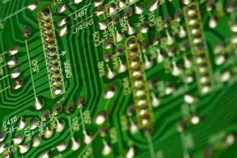
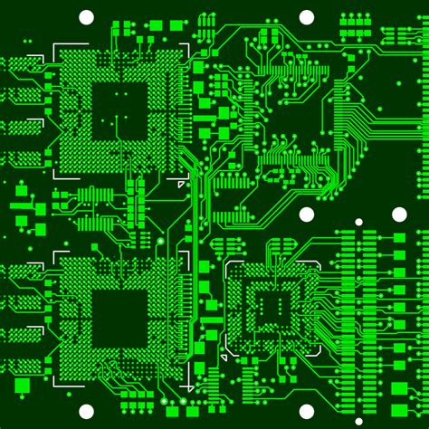
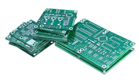
A printed circuit board, or PCB, is a flat board made of insulating material like fiberglass, with conductive copper tracks printed onto it in a specific pattern. Electronic components like resistors, capacitors, microchips, and connectors are soldered onto the PCB to create a complete circuit.
PCBs provide mechanical support and electrically connect the various components using the conductive tracks, pads, and other features etched from copper sheets laminated onto a non-conductive substrate. They are used in almost all electronic devices and equipment today.
Types of PCBs
There are several different types of printed circuit boards:
| PCB Type | Description |
|---|---|
| Single-sided | Conductive copper tracks printed on one side of the board only |
| Double-sided | Conductive tracks on both sides of the board, with through-hole connections |
| Multi-layer | Multiple double-sided PCBs sandwiched together with insulating layers in between |
| Rigid | Made from solid substrate material that prevents the board from flexing |
| Flex | Uses flexible high-temperature plastic as the insulating material to allow bending |
| Rigid-flex | Combines rigid and flexible sections in a single board |
The type of PCB used depends on the specific requirements of the device or application in terms of size, complexity, operating environment, etc.
The PCB Design process
Developing a new printed circuit board involves several steps in the design process:
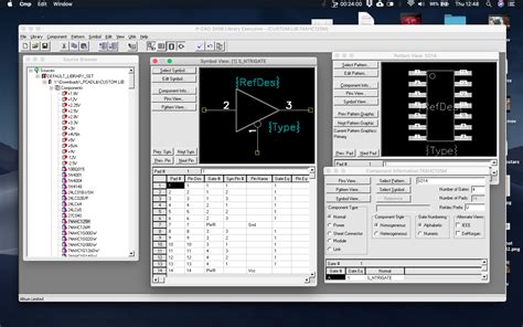
1. Schematic capture
The first step is to create a schematic diagram that defines the interconnections between components. This is typically done using electronic design automation (EDA) software. The schematic captures the logical connections without specifying the physical layout.
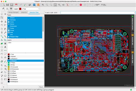
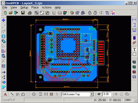
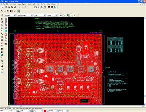
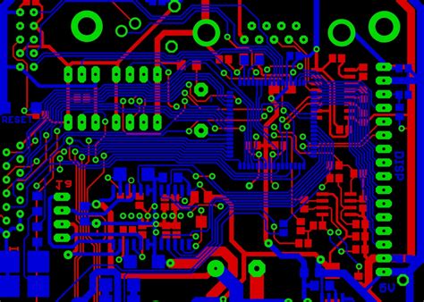
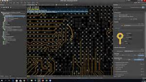
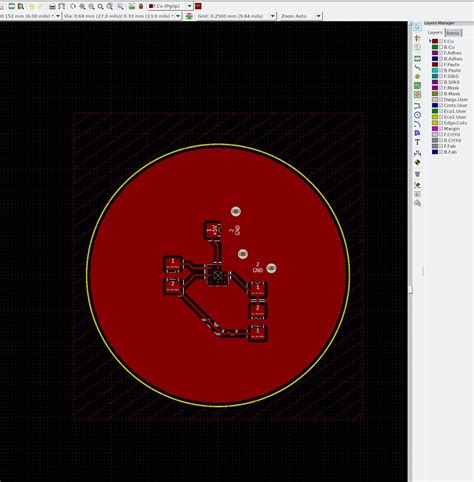
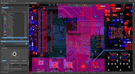
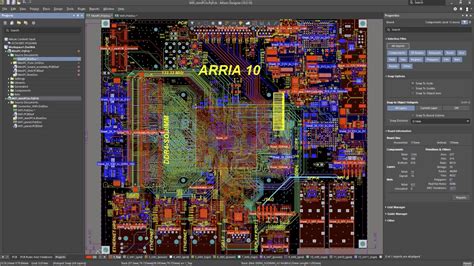
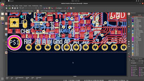
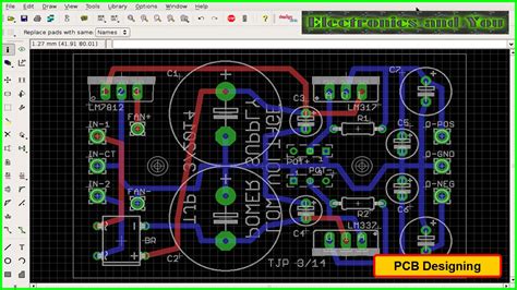
2. Board layout
Next, the PCB layout is created based on the schematic. Components are arranged on the board and conductive tracks are routed to make the required connections. The physical size and shape of the board are defined. Layers, ground planes, hole drilling, and other fabrication aspects are specified.
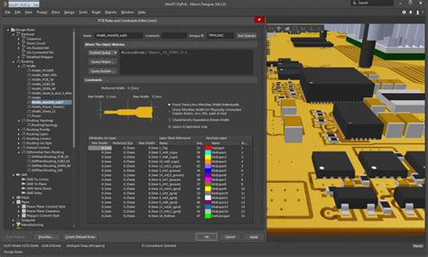
3. Design rule checks
The layout must be checked to ensure it meets the PCB manufacturer’s design rules in terms of minimum trace width/spacing, hole sizes, clearances, etc. EDA software includes design rule checks (DRC) to verify the layout.
4. Outputting files
Once the layout is finalized, the design files are output in the format required by the PCB manufacturer. Gerber files are the industry standard for defining the copper layers, solder mask, legend, and drill holes. The bill of materials (BOM), assembly drawings, and other documentation are also generated.
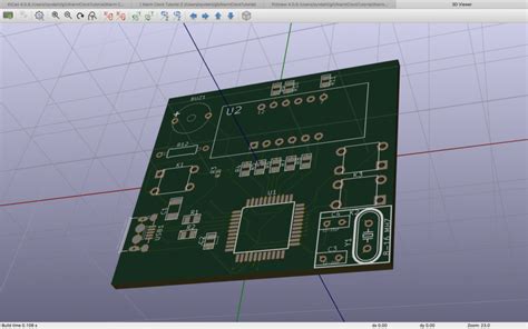
5. Prototyping and testing
A prototype of the PCB is fabricated and assembled. It undergoes thorough testing and debugging to verify the design and fix any issues. The prototype may go through several revisions before the design is finalized for production.

PCB design considerations
Designing a printed circuit board involves balancing many different requirements and constraints. Some key considerations include:
Component selection and placement
The types and sizes of components used will impact the PCB layout. They must be selected and placed in a way that minimizes the board size while allowing adequate space for routing traces. Component parameters like power dissipation and high-frequency effects must also be considered.
Signal integrity
Maintaining signal integrity is critical, especially in high-speed designs. This involves ensuring proper trace impedance, minimizing crosstalk, and avoiding reflections. Techniques like differential pairs, ground planes, and smoothly routed traces are used to preserve signal quality.
Power integrity
The PCB must provide a clean, stable power supply to all components. This requires proper power plane design, decoupling, and filtering. The power distribution network (PDN) must have low impedance and be free of voltage droops or ripple.
Electromagnetic compatibility (EMC)
The PCB must not emit excessive electromagnetic interference (EMI) that could disrupt nearby devices. It must also have immunity to external EMI. Techniques like shielding, filtering, and proper grounding are used to ensure EMC.
Thermal management
High-power components generate significant heat that must be dissipated to avoid overheating. The PCB layout must provide adequate thermal relief through proper component placement, copper pours, and heatsinks if needed.
Manufacturing considerations
The PCB design must be manufacturable using standard fabrication and assembly processes. This means adhering to the manufacturer’s design rules and leaving room for test points and fiducials. Panelization and assembly considerations should be taken into account.

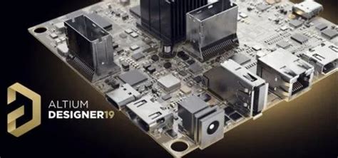
PCB design software tools
PCB design is done using specialized electronic design automation (EDA) software. Some of the leading PCB design tools include:
| Tool | Vendor |
|---|---|
| Altium Designer | Altium |
| OrCAD | Cadence Design Systems |
| PADS | Mentor Graphics (Siemens) |
| Xpedition | Mentor Graphics (Siemens) |
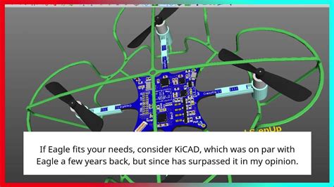
| EAGLE | Autodesk |
| KiCad | Open-source |
These tools provide schematic capture, board layout, routing, simulation, and output generation capabilities. They include extensive component libraries, design rule checks, and interfaces to manufacturing tools and processes.
Career opportunities in PCB design
PCB design is a growing field with strong demand for skilled engineers. Some career opportunities include:
PCB designer
PCB designers create the board layouts using EDA software. They work closely with electrical engineers to implement their schematic designs and with mechanical engineers on the physical housing.
Electrical engineer
Electrical engineers define the circuit design and specify the components and interconnections. They create the schematics that drive the PCB layout.
Electronics packaging engineer
Packaging engineers integrate the PCB into the complete product assembly. They ensure the PCB fits in the housing and interfaces with other components like displays and connectors.
Manufacturing engineer
Manufacturing engineers take the PCB design and develop the fabrication and assembly processes to mass produce the board in a factory setting.
Signal/power integrity engineer
SI/PI engineers specialize in analyzing and optimizing high-speed designs. They perform simulations to verify signal quality and power delivery network performance.
Frequently asked questions (FAQ)
What is the difference between a schematic and a PCB layout?
A schematic defines the logical connections between components without specifying the physical arrangement. The PCB layout determines the actual physical placement of components and routing of traces on the board.
What are vias in a PCB?
Vias are small holes drilled in a PCB to route a trace from one layer to another. They are plated with metal to provide electrical conductivity between layers.
What is a ground plane?
A ground plane is a large area of copper on a PCB layer that provides a low-impedance return path for currents. It helps reduce EMI and maintains signal integrity.
What are the different types of PCB components?
PCB components can be broadly classified as through-hole (inserted into holes drilled in the board) or surface-mount (soldered directly onto pads on the surface of the board). Examples include resistors, capacitors, integrated circuits, connectors, and switches.
How are PCBs manufactured?
PCBs are fabricated by laminating copper foil onto an insulating substrate material. The copper is selectively etched away to form the traces and pads. Layers are aligned, laminated together, and holes are drilled. The board is then plated, solder mask and silkscreen are applied, and the boards are routed or V-scored out of a panel.
Conclusion
PCB design is a complex process that requires knowledge of electronics, materials, manufacturing processes, and specialized software tools. A well-designed PCB is critical to the proper functioning and reliability of any electronic device.
As electronics continue to become more pervasive and sophisticated, the demand for skilled PCB designers will only increase. It is a challenging but rewarding field that offers many opportunities for career growth and advancement.