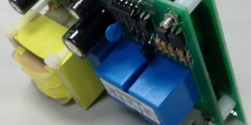
During PCBA wave soldering, solder spatter may occur on the solder surface of the PCB and on the component surface. It is commonly believed that if water vapor remains on the PCB before it enters the wave, once it comes into contact with the solder on the wave, it will quickly evaporate into steam within a very short period of time at high temperatures. Up, resulting in an explosive exhaust process. It is this intense exhaust that can cause a small explosion inside the solder seam in the molten state, resulting in particles of solder escaping from the seam and thus splashing onto the PCB. Conclusion:
manufacturing environment and PCB storage time
The manufacturing environment has a significant impact on the solder quality of electronic components. High humidity in the manufacturing environment, long periods of PCB packaging and opening for SMT placement process and PCBA wave soldering production, or PCBA wave soldering after a period of PCB placement, insertion, all these factors may produce tin beads in the PCBA wave soldering process.
If the manufacturing environment is too humid, in the product manufacturing process will be easy to accumulate water on the surface of the PCB floating in the air condensation, condensation of water, in the PCB hole, when the PCBA wave soldering, preheating temperature area in the hole will have fine droplets of water may not be fully completed, these will not evaporate, water droplets will be in contact with the PCBA wave soldering, bear high temperature, steam will evaporate in a short time, but now is the time to form a solder joint, the water vapor will create voids in the solder, tin or extruded solder balls. In severe cases, an explosive spot is formed, surrounded by tiny beads of blown tin.
If the PCB in the package is opened for a long time after the PCBA wave soldering, there will also be condensation beads in the through-hole; after the completion of the placement or cartridge, the PCB will also condense after sitting for a period of time. For the same reason, these beads will lead to the formation of solder beads during PCBA wave soldering.
Therefore, as a company engaged in SMT patch processing, the requirements of the manufacturing environment and the timing of the product manufacturing process are particularly important. The PCB should be inserted and soldered within 24 hours after the patch is completed. If the weather is dry, it can be done within 48 hours.
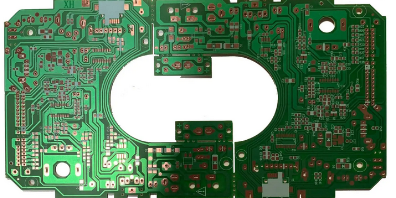
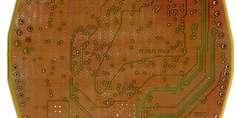
PCB resistance welding materials and production quality
Solder film used in PCB manufacturing is also one of the reasons for tin balls in PCBA wave soldering. As the solder film and flux have a certain degree of affinity, the processing of the solder film often leads to the attachment of solder beads, which leads to the generation of solder balls.
PCB manufacturing quality is poor will also produce tin balls in the PCBA wave soldering process. If the PCB through-hole hole wall coating is thin or there are gaps in the coating, the water attached to the PCB through-hole will be heated to steam, the water vapor will be discharged through the hole wall, and the solder will produce solder balls. Therefore, the appropriate coating thickness in the through-hole is very critical.
When there is dust or dirt in the PCB via hole, the flux sprayed into the via hole will not get enough volatiles in the PCBA wave soldering process, and the liquid flux (such as water vapor) will also produce tin beads when it encounters the wave.
Correct selection of flux
There are many reasons for solder balls, but flux is the main reason. General low solid content, no-clean flux is more likely to form solder balls, especially when the bottom surface of the SMD components need to double PCBA wave soldering, this is because these additives are not designed to be used for a long time. If the flux sprayed on the PCB after the first wave has been used up, there is no flux after the second wave, so it can not function as a flux and help reduce solder balls. One of the main ways to reduce the number of solder balls is to choose the right flux. Choose a flux that can withstand heat for a longer period of time.
Shenzhen RayMing is an electronic product processing company specializing in SMT chip processing, DIP plug-in processing, PCBA package, PCB circuit board manufacturing, with 16 years of experience in electronic processing, as well as advanced production equipment and perfect after-sales service system. Welcome new and old customers to call us!