Judy@4pcba.com
7:30 AM - 7:30 PM
Monday to Saturday

Archive: July 31, 2023

Nuvoton W78E052DFG Microcontroller Decryption

Nuvoton W78E052DFG Microcontroller Decryption

RayMing successfully cracked Nuvoton W78E052DFG MCU, and now provides W78E052D chip decryption and other Nuvoton MCU decryption, Winbond MCU decryption, and Huabang chip program extraction services for domestic and foreign customers.

W78E052D Overview:
The W78E052D is an 8-bit microcontroller that accommodates a wider frequency range with low power consumption.The instructions of the W78E052D family of microcontrollers are fully compatible with those of the standard 8051.
The W78E052D contains 8K bytes of Flash ROM for updating the load program, 256 bytes of RAM, four 8-bit bi-directional (P0, P1, P2, P3), bit-addressable I/O ports, an additional 4-bit I/O port P4, three 16-bit timers/counters, a hardware watchdog timer, and serial port. All of these peripherals support 8-source, 4-level interrupt capability. For easy programming and verification, the flash EPROM inside the W78E054D/W78E052D/W78E051D series allows program memory to be programmed and read electronically. Once the code is verified, the user can protect the security of the code.

W78E052D Features:
-Full static design 8-bit CMOS microcontroller.
-Selectable 12T or 6T mode
􀂄12T mode, operates every 12 clock machine cycles (default) at speeds up to 40 MHz/5V
􀂄6T mode, operating every machine cycle set by the writer, with clock speeds up to 20 MHz/5V
-Wide supply voltage of 2.4V to 5.5V
-Temperature grade (-40°C to 85°C)
-Pin and instruction set compatible with MCS-51
-256 bytes of on-chip staging RAM
-16K/8K/4K bytes of electrically erasable/programmable Flash EPROM.
-2K bytes of LDROM to support ISP function (refer to application notes)
-64KB program memory address space
-64KB data memory address space
-4 8-bit bi-directional ports
-8 sources, 4 levels of interrupt capability
-An additional 4-bit bit-addressable I/O port, additional INT2/ INT3 (PQFP, PLCC and
LQFP packages)
Three 16-bit timers/counters
One full-duplex serial port
-Watchdog timer
-EMI reduction mode
-Software reset
-Built-in power management idle and power-down modes
-Code protection
-Package:
W78E052DDG DIP-40 Pin -40oC~85oC
W78E052DPG PLCC-44 Pin -40oC~85oC
W78E052DFG PQFP-44 Pin -40oC~85oC
W78E052DLG LQFP-48 Pin -40oC~85oC

dsPIC30F5015 microcontroller decryption price reduction offer dsPIC30F chip decryption short cycle time

dsPIC30F5015 microcontroller decryption price reduction offer dsPIC30F chip decryption short cycle time

RayMing Technology dsPIC30F5015 microcontroller decryption program is mature, our dsPIC30F2010, dsPIC30F3010, dsPIC30F4012, dsPIC30F3011, dsPIC30F4011, dsPIC30F5015, dsPIC30F6010 and dsPIC30F6010A and other dsPIC30F series chip decryption price is low, and the cycle of MCU crack short. If you have dsPIC30F5015 chip decryption or other dsPIC30F microcontroller decryption needs, welcome to call and visit us.

dsPIC5015 device performance profile:
High performance modified RISC CPU:
-Improved Harvard architecture
-C compiler optimized instruction set architecture
-Flexible addressing mode 84 basic instructions
-24-bit wide instructions, 16-bit wide data
12 KB on-chip flash program space
-512 bytes of on-chip data RAM
-1 byte of non-volatile data EEPROM
-16 x 16-bit operating register array
-Up to 30 MIPS operation:

  • DC to 40 MHz external clock input
  • 4 MHz, 10 MHz with PLL active (4x, 8x, 16x) oscillator inputs
    -27 interrupt sources
    -Three external interrupt sources
    8 user-selectable priority levels per interrupt
    -4 processor exceptions and software traps
    DSP engine features:
    -Mode and bit inversion modes
    -Two, 40-bit wide accumulators with optional saturation logic
    -17-bit x 17-bit single-cycle hardware decimal/integer multiplier
    -Single-cycle multiply-accumulate (MAC) operation
    -40-level barrel shift
    -Double fetch data
    Peripheral Characteristics:
    -High sink/pull current source I / O pins: 25 mA/25 mA.
    Three 16-bit timers/counters; 16-bit timer into 32-bit timer module
    4 16-bit capture input functions
    2 16-bit compare/ PWM output functions
  • Dual compare mode available
    -3-wire SPITM module (supports 4-frame mode)
    -I2CTM module with multi-mode and 7-bit/10-bit resolution support
    -Addressable UART module with FIFO buffer
    Motor control PWM module features:
    -6 PWM output channels
  • Complementary or independent output modes
  • Edge and center aligned modes
    -4 duty cycle generators
    -Dedicated 4-mode time base
    -Programmable output polarity
    -Dead complementary mode time control
    -Manual output control
    -Trigger synchronized A/D conversion
    Quadrature Encoder Interface Module Features:
    -Phase A, phase B and index pulse inputs
    -16-bit up/down position counter
    -Counting direction status
    -Position measurement (x2 and x4) modes
    -Programmable input digital noise filter
    -Alternate 16-bit timer/counter mode
    -Interrupt/underflow position counter flip-flop
    Analog Features:
    -10-bit analog to digital converter (A/D) with:
  • 500 ksps (10-bit A/D) conversion rate
  • 6 input channels
  • Conversion is available at sleep and idle
    -Programmable undervoltage detection and generation reset.

The dsPIC30F devices contain a high-performance 16-bit microcontroller (MCU) architecture with extensive digital signal processor (DSP) functionality inside. Based on the widespread use of dsPIC30F2010, dsPIC30F3010, dsPIC30F4012, dsPIC30F3011, dsPIC30F4011, dsPIC30F5015, dsPIC30F6010 and dsPIC30F6010A dsPIC30F series microcontrollers, the The demand for dsPIC30F crack is also increasing. Hualan Technology is pleased to offer dsPIC30F2010, dsPIC30F3010, dsPIC30F4012, dsPIC30F3011, dsPIC30F4011, dsPIC30F5015, dsPIC30F6010, dsPIC30F6010A, etc. dsPIC30F series chips for cracking with reduced price. Preferential activities.

SN8P2714KB chip decryption program mature RayMing specializes in the decryption of Song Han SONIX microcontroller

SN8P2714KB chip decryption program mature RayMing specializes in the decryption of Song Han SONIX microcontroller

RayMing Technology specializes in decryption of SONIX microcontrollers in Songhan, and our SONIX chip decryption program is mature. Our SONIX chip decryption program is mature. We can complete the decryption of Songhan SN8P2714KB chip within a few hours and guarantee the success rate is 100%.
Now for domestic and foreign customers to provide favorable price Song Han SN8P2714KB chip decryption, and other series of SONIX microcontroller cracking services.

SN8P2714 is Taiwan SONIX 8-Channel 12-bit ADC, High speed (1T), High EFT protection.

SN8P2714 has a RISC-like high performance and low power consumption system. 1T (one instruction cycle is one clock) architecture, 16MIPS computing power. In addition, the high EFT performance makes it suitable for applications in high-interference industrial environments.The SN8P2714’s top-notch IC architecture includes 2K-word program memory (OTP ROM), 128-byte data memory (RAM), two 8-bit time counters (TC0, TC1), a watchdog timer, four interrupt sources (TC0, TC1, INT0, INT1), and an interrupt source (INT0, INT1). INT0, INT1), 7-bit DAC converter, 8-channel 12-bit ADC converter, 2-channel PWM outputs (PWM0, PWM1), buzzer outputs (BZ0, BZ1), and 8 levels of stack buffer.The SN8P2714 provides 4 different oscillator modes for the system to serve as the system clock, including high/low speed crystal oscillator, ceramic resonators and inexpensive RC oscillators. In addition, the SN8P2714 includes a programmable internal low-frequency RC oscillator as the clock source for the low-speed mode.

SN8P2714KB Chip Characteristics:
Operating voltage: 2.4V~5.5V (Fosc = 4MHz)
ROM: 2K * 16 bits
RAM: 128 * 8 bits
8-level stack buffer
Unidirectional input pin: P0
Bidirectional input and output pins: P2, P4, P5
Wake-up port triggered by level change: P0
P4 pin shared with ADC
External interrupt source: P0
Two external interrupt sources: INT0, INT1
Two internal interrupt sources: TC0, TC1
Built-in watchdog timer
8-channel 12-bit ADC
1 channel 7-bit DAC
External high-speed clock: crystal 16MHz maximum
Internal low-speed clock: RC oscillator, 16KHz/3V, 32KHz/5V
One clock cycle is one instruction cycle
Most instruction cycles are one cycle
Table lookup function (MOVC) addresses the entire ROM area

ATMEGA3290 chip decryption and ATMEGA6490 microcontroller decryption successfully

ATMEGA3290 chip decryption and ATMEGA6490 microcontroller decryption successfully

ATMEGA329 and ATMEGA3290 are with 32K bytes of in-system programmable FLASH memory, and ATMEGA649 and ATMEGA6490 are with 64K bytes of in-system programmable FLASH memory.RayMing Technology ATMEGA329, ATMEGA3290, ATMEGA649 and ATMEGA6490 MCU decryption solutions are mature and can ensure that the chip decryption is completed within hours and the success of chip decryption is 100%. ATMEGA6490 microcontroller decryption of the program is mature, can ensure that the chip decryption in a few hours to complete, and chip decryption success rate of 100%.

Characterization of ATMEGA329, ATMEGA3290, ATMEGA649 and ATMEGA6490:
-High-performance, low-power 8-bit AVR® microcontrollers
-Advanced RISC architecture

  • 131 instructions – most of them executed in a single clock cycle
  • 32*8 general-purpose working registers
  • Fully static operation
  • Up to 20 MIPS throughput at 20 MHz
  • On-chip 2-cycle multiplier
    Highly durable, non-volatile memory segments
  • 32K bytes of in-system programmable Flash (ATMEGA3290)
  • 1024 bytes of EEPROM (ATMEGA3290)
  • 2K bytes of on-chip SRAM (ATMEGA3290)
  • Write/erase count: 10,000/ 10,000 times EEPROM
  • Data retention: 20 years at 85°C / 100 years at 25°C (1)
  • Optional boot with independent locking of bit code segments, on-chip bootloader programmed in the system, true simultaneous read and write operations
  • Programming software security lock
    -Peripheral Features
  • Two 8-bit timer/counters with independent prescaler and compare modes
  • One 16-bit timer/counter with independent prescaler, compare mode, and capture mode
  • Real-time counter with independent oscillator
  • 6 PWM channels
  • 8-channel 10-bit ADC for temperature measurement in TQFP and QFN/MLF packages
  • 6-channel 10-bit ADC pin PDIP package temperature measurement
  • Programmable Serial USART
  • Master/Slave mode SPI serial interface
  • Byte-oriented two-wire serial interface (Philips I2C compatible)
  • Programmable watchdog timer with independent on-chip oscillator
  • On-chip analog comparator
  • Interrupt and wake-up pin level changes
    -Special processor features
  • Power-on reset and programmable power-down detection
  • Internally calibrated oscillator.
  • External and internal interrupt sources
  • 6 sleep modes: Idle Mode, ADC Noise Suppression, Power Save, Power Down, Standby, Extended Standby
    -I/O and Packaging
  • 54/69 programmable I/O lines
  • 64-lead TQFP, 64-pad QFN/MLF, and 100-lead TQFP
    -Operating voltage:
  • ATmega329PV: 0 – 4 MHz @ 1.8 – 5.5V, 0 – 10 MHz @ 2.7 – 5.5V
  • ATmega329P:0 – 10 MHz @ 2.7 – 5.5V, 0 – 20 MHz @ 4.5 – 5.5V
    -Temperature range: -40°C to 85°C.
    -Low power frequency is:
  • Active Mode:420°C at 1 MHz, 1.8V
  • Power-down Mode:40 nA at 1.8V
  • Power-save Mode:750 nA at 1.8V

If you have ATMEGA329, ATMEGA3290, ATMEGA649 and ATMEGA6490 chip decryption needs, you can call and visit us to discuss, we provide the industry’s lowest price ATMEGA329, ATMEGA3290, ATMEGA649 and ATMEGA6490 chip cracking service and other AVR series Microcontroller decryption services.

Exclusive Core MIKKON chip decryption MK7A23P and MK7A25P microcontroller decryption

Exclusive Core MIKKON chip decryption MK7A23P and MK7A25P microcontroller decryption

RayMing Technology exclusively provides Taiwan VIVOTEK MIKKON chip decryption, whether it is a package or bonding chip, we can successfully complete the chip crack.
Core MIKKON chip applications: home appliance control, computer peripherals, induction cookers, various types of chargers, mobile power, UPS power supply, electric kettle, electric pressure cooker, rice cooker, LED, toys, remote control, LCD electronic clock, perpetual calendar, therapeutic instrument, air conditioning remote control, game consoles, USB sound card, USB small digital photo frame, U disk, card reader and other data speed transmission requirements for fast products and so on. The data transfer speed is required to be fast, etc.

Due to the high performance and low price of VIVOTEK microcontrollers and compatible with many brands of IC feet, VIVOTEK microcontrollers are widely used. Therefore, the market demand for VIVOTEK MIKKON chip decryption is also more and more, RayMing Technology after in-depth technical research to successfully obtain the VIVOTEK MIKKON chip decryption program. Now, we provide Taiwan VIVOTEK microcontroller decryption, MIKKON chip decryption exclusively.

RayMing Technology Taiwan Core MIKKON chip decryption high success rate and low price.

Core 8-bit microcontroller model:
MK7A10P (compatible with EM78P153/156/447/SN8P2501/PIC12C508/54/57).
MK7A20P(Compatible with PIC16F57/EM78P447).
MK6A20P.
MK6A12DP.

VIVOTEK 8-bit ADC Microcontroller Models:
MK7A21P (HT46R47 compatible); MK7A21P (HT46R47 compatible); MK7A22P (HT46R47 compatible)
MK7A22P (S3F9454 compatible); MK7A23P (S3F9454 compatible); MK7A23P (S3F9454 compatible)
MK7A23P (compatible with S3F9454); MK7A25P; MK7A25P; MK7A25P; MK7A25P
MK7A25P.

VIVOTEK 8-bit LCD Microcontroller Models:
MK9A35P (EM78P468 compatible); MK9A50P; MK7A25P; MK7A25P; VIVOTEK 8-bit LCD Microcontroller Models.
MK9A50P.
MK9A80P; MK9A160P
MK9A160P.

VIVOTEK USB Controller Models:
MK8A03BP(Compatible with HT82A523R, EM78P680);; MK9A50P; MK9A80P; MK9A160P; VIVOTEK USB Controller Model.

RayMing Technology corex microcontroller decryption service efficiency and low price, whether it is a package chip or bonding chip, we can successfully complete the chip crack. We can successfully complete the chip cracking. We are your first choice service provider for Core MIKKON chip decryption.

Renesas M30843FJGP chip decryption,RENESAS chip decryption

Renesas M30843FJGP chip decryption,RENESAS chip decryption

M30843FJGP is a member of Renesas MC32C/84 series microcontrollers, which is a single chip control unit with MC32C/84 series CPU core using high performance silicon gate CMOS technology.
For Renesas MC32C/84 series microcontroller M30843FJGP chip decryption, RayMing Technology has made a major breakthrough after a long time of technical research, and now provides favorable price M30843FJGP chip decryption and other MC32C/84 series RENESAS MCU decryption.

M30843FJGP and MC32C/84 series RENESAS microcontrollers are mainly used in automobiles, stereos, cameras, office equipment, communication equipment, portable devices and so on.

M32C/84 series microcontrollers are as follows:
M30840MC-XXXFP, M30840MC-XXXGP,M30840SFP, M30840SGP, M30842MC-XXXGP, M30842SGP;  
m30843fhfp,m30843fhgp,m30843fjfp,m30843fjgp,m30843fwgp,m30843mw-xxxfp,m30843mw-xxxgp; 
m30845fhgp,m30845fjgp,m30845fwgp,m30845mw-xxxgp,m30840mct-xxxgp,m30842mct-xxxgp; m30843fjtgp,m30843fjtgp,m30843mgt-xxxgp,m30843mgu- XXXGP,M30843MHT-XXXGP;
m30843mhu-xxxgp,m30843mwt-xxxgp,m30843mwu-xxxgp,m30845fhugp.

Features of M30843FJGP:
1) 16-bit multi-function timer (Timer A and B, including 3-phase inverter motor control function): 11 channels
2) Input Capture/Output Compare Timer (Timer S): 16 bits x 1 channel
3) UART/Clock Synchronized Serial Interface: 6 channels
4) Multi-master I2C bus interface: 1 channel
5) USB: Full Speed (12 Mbps, compliant with USB 2.0 specification)
6) 10-bit A/D converter: 2 circuits, 26 channels
7) 8-bit D/A converter: 2 channels
8) DMAC: 4 channels
9) CRC calculation circuit
10) Watchdog Timer
11) Clock generator: main clock, sub-clock, internal oscillator (high speed/low speed), PLL frequency synthesizer
12) Oscillation stop detection
13) real-time clock
14) voltage detector
15) Power-on reset
16) I/O port: 85
17) External Interrupt Input: 13
18) Data Flash: 4KB × 2 blocks

Renesas HD64F2339VFC25 Chip Decryption,Hitachi H8S2339 Chip Cracking

Renesas HD64F2339VFC25 Chip Decryption,Hitachi H8S/2339 Chip Cracking

HD64F2339VFC25 is a member of Renesas H8S series microcontrollers. For Renesas H8S/2339 microcontroller HD64F2339VFC25 chip decryption, RayMing Technology has made a significant breakthrough after a long time of technical research, and now provides HD64F2339VFC25 chip decryption at favorable prices and other H8S series RENESAS MCU decryption.

H8S series chips are introduced as follows:
This is a rich product line to fit your application. High-speed operation, 3V/5V-I/F hybrid, low-voltage operation and USB, CAN, IE bus, equipped with a variety of interfaces suitable for Ethernet, LCD and other applications, will meet a variety of customer needs.

  1. adopting static circuit, 16-bit high-end model;.
  2. Minimum instruction execution time of 30ns is realized when basic instruction is 3.3V/33MHz in one state;.
  3. 2.2V low voltage running goods also queued; 4.
  4. Compared with conventional 16-bit microcontrollers, low-power processing of less than 1/5 in performance and functionality is realized.
  5. Compared with traditional low-noise products, low-noise products can reduce unnecessary noise width deformation by 10~20db.
  6. H8/300, H8/300H and upward compatible instructions

Features of HD64F2339VFC25:
Memory
Program memory: Flash memory
CPU (Bit, Clock, DMA, External Bus etc)
CPU: H8S/2000 (16-bit)
Max. Frequency: 25 MHz
External Interrupt Pins: 9
Timers
8-bit Timers: 2 ch
16-bit Timers: 6 ch
Watchdog Timers: 1 ch
A/D Converters: 10-bit x 12 ch
D/A Converters: 8-bit x 4 ch
Operating Conditions
Operating Temperature: -40 to 85 °C

PCB copy board of Protel 99SE copper laying problem summary

PCB copy board of Protel 99SE copper laying problem summary

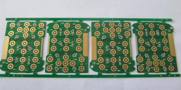
In PCB copy board or PCB design, we often encounter some copper laying problems. The following is a summary of these issues:
First, what is the role of copper laying in PCB circuit board placement?
Heat dissipation;
Shielding Anti-interference pcb board with parasitic capacitance;
Improve the strength of the board;
Aesthetics;
Increase the difficulty of being copied boards, especially copper + black oil.

Second, PROTEL irregular copper laying method:
1, first of all, we need to know in the PCB that piece of area to lay copper
2, and then determine the need to pave the copper of the region Shop what kind of network of copper (to determine what power supply, or what ground, or what other networks)
3, click on the tool to lay copper
4, set the copper paving safety spacing and line width and grid spacing
5, set the way to lay copper (positive, diagonal grid)

Third, laying copper settings

Net Option group: set the network to be connected by copper-laying, mainly containing three options
Connect to net: set the name of the network to which copper is to be connected, if you choose No Net, the 2 options below the list are meaningless.
Pour Over Same: override the same network name, i.e. if you choose GND as the copper connection, even if you draw some ground lines on the PCB, these ground lines will be overridden when laying copper. If you don’t select this item, the ground lines that have already been drawn will not be overwritten.
Remove Dead Copper: Remove Dead Copper, some isolated, not connected to the GND of the circuit of the copper is known as dead copper or lonely copper, these copper can only be used to decorate the PCB, not a lot of practical significance.

Hatching Style: set the way to lay copper, respectively, to 90 degrees, 45 degrees, vertical, horizontal way of copper film alignment settings.

Plane Settings: Set the grid point interval of copper film line.
Grid Size: Set the spacing of copper polygon, i.e. copper density.
Trace Width: set the width of the copper film line.
Layer: Set the layer where the copper is laid.
LockPrimitves: lock all the copper, generally check it.
If the line width is greater than the grid spacing, then the PCB board of copper is the whole piece of copper skin.

Surround Pads With: set the copper and pads between the surround mode, 8-edge type or arc surround

Minimun Primitives Size: set the shortest length of the copper film line, the larger the value, the faster the speed of laying copper.

Note: In wiring, the minimum line width (Track Width) can not be less than 0.01, Grid Size (Grid Size) can not be less than 0.01. If you find a mistake in the copper laying process, you can press Backspace to delete the drawn shape.

If you want to keep more copper paving area, we usually do not set Delete Dead Copper to be effective as soon as we start paving copper, in that case, you will see a large piece after paving, a large piece of spare space is not paved. So first directly lay, after laying, observe those are dead copper, see if you can try to connect through the upper and lower layers of copper. If there is really difficult to connect individual places, see if you can optimize the PCB, try to save the dead copper through the hole. If there is no other way, we can choose to remove the dead copper items and resurface the board to make it more neat and tidy.

Sometimes we want to pad wires, etc., away from the copper film line a little farther, we need to set up RULE in the distance between the distance, if we increase the distance between the distance, the system may prompt a lot of ERC detection errors, but it does not matter, and so we pave the copper after the completion of the distance between the distance to set back to the good.

If you want to keep more copper laying area, we usually don’t set Delete Dead Copper to be effective as soon as we start laying copper, in that case, you will see a big piece after laying, a big piece of free space is not laid. So first directly lay, after laying, observe those are dead copper, see if you can try to connect through the upper and lower layers of copper. If there is really difficult to connect individual places, see if you can optimize the PCB, try to save the dead copper through the hole. If there is no other way, we can choose to remove the dead copper items and resurface the board to make it more neat and tidy.
Sometimes we want to pad wires, etc., away from the copper film line a little farther, we need to set up RULE in the distance between the distance, if we increase the distance between the distance, the system may prompt a lot of ERC detection errors, but it does not matter, and so we pave the copper after the completion of the distance between the distance to set back to the good.

Fourth, protel99 copper pavement deletion
shortcut key E + D, and then to delete the cloth copper on the mouse point. Or use the network selection method, select the network to delete, and then delete.
protel99 can delete part of the copper pavement? It is to cut off a piece of the existing copper lay that is not wanted. After I laid the wires and copper, I found that there is some problem to change the wiring, so the copper should be changed, but I don’t want to delete all the wires and change them and then re-lay them again, because it’s an irregular copper, which is more troublesome. Delete to change the place to lay copper, change and then lay on a good operation.

Fifth, protel99 copper paving modification
When you find that the copper is not satisfactory, or need to change the alignment again, you had better delete the copper, after the change, and then lay once. The method of deletion is to use the delete command under the editor, the mouse will be in the state of the delete command, click on the copper on the deletion of the store, than some of the books introduced to adjust the effect of copper on the store much better.

Simple single-panel copy board and double-panel copy board method

Simple single-panel copy board and double-panel copy board method

The difference between a single panel and a double panel is that a single panel has wiring on one side only, while a double panel has wiring on both sides. Double-sided board is an extension of the single-panel, meaning that the single-panel line is not enough so as to turn to the opposite side of the double-sided board is also an important feature is that there are through-holes. Therefore, the method and steps of double-sided board copying are similar to those of single-sided board copying.

Simple single panel copy board and double-sided board copy board steps:
1, scan the upper and lower layers of the circuit board, save two BMP pictures.
2, open the board copying software Quickpcb2005, point “file” “open the bottom picture”, open a scanned picture. With PAGEUP to enlarge the screen, see the pad, according to PP to place a pad, see the line according to the PT line …… like a child tracing the same, in this software tracing again, point “Save” to generate a B2P file.
3, and then point “file” “open the bottom of the map”, open another layer of scanning color map; 4, and then point “file” “open the bottom of the map”, open another layer of scanning color map.
4, and then point “File” “Open”, open the previous saved B2P file, we see just copied the board, stacked on top of this picture – the same PCB board, holes in the same location, just different line connections. The same PCB board, holes in the same location, just different line connections. So we press the “Options” – “Layer Settings”, where the display of the top layer off the line and silkscreen, leaving only multi-layer vias.
5, the top layer of perforations and the bottom layer of the picture on the same location of the perforations, and now we like childhood tracing the same, tracing the bottom layer of the line can be. Then point “Save” – this time the B2P file will have a top and bottom of the two layers of information.
6, point “File” “Export as PCB file”, you can get a PCB file with two layers of information, you can then change the board or schematic or directly to the PCB plate factory production.

Single and double-sided board copying is the simplest and most common circuit board copying in PCB copying, RayMing Technology single and double-sided board copying is completed within 1 day, the success rate is 100%.

Four-layer board copying and multilayer board copying methods and techniques

Four-layer board copying and multilayer board copying methods and techniques

Four-layer board copying is to repeat the copying of two double-sided boards, six-layer board copying is to repeat the copying of three double-sided boards, and so on, and multilayer board copying is to repeat the copying of multiple double-sided boards. The reason why multilayer is so daunting is that we can’t see the internal alignment.

So how can we see the inside of a multilayer board? This problem can be solved by layering. Now there are many ways to delamination, there are potion corrosion, tool stripping, etc., but it is easy to layer overload, loss of information. Experience tells us that sandpaper is the most accurate method of layering. Grinding board is currently the most common layering program, but also the most economical.

When we complete the top and bottom of the multilayer PCB board copy board, sandpaper sanding method to grind off the PCB surface layer to show the inner layer. Sandpaper is a hardware store to sell ordinary sandpaper, generally flat PCB, and then hold down the sandpaper, evenly rubbed on the PCB (if the board is very small, you can also lay the sandpaper, with a finger to hold down the PCB in the sandpaper rubbing). The main point is to lay flat, so as to grind evenly. Silk screen and green oil is generally a wipe off, copper wire and copper skin should be well rubbed a few times. General Bluetooth board a few minutes to wipe well, memory sticks about ten minutes.

Four-layer board copy board method steps:
1, scanning the top and bottom of the four-layer circuit board picture;
2, to complete the top and bottom of the four-layer circuit board copy board work;
3, sandpaper sanding off the top and bottom of the four-layer circuit board, revealing the inner two layers of the four-layer board;
4, scanning the four-layer circuit board inside the two layers;
5, in the board copying software to add the middle layer, and complete the four-layer circuit board inside the two layers of the board copying work;
6, four-layer board copy board work is completed, respectively, check each layer of the line to ensure the accuracy of the PCB copy board.

Multi-layer board copying method steps with reference to the four-layer board copying method analogous. The more layers of the board, the greater the workload of PCB copying.

Multilayer board copying skills:
After the completion of multilayer board copying, the cost of PCB board making is several times that of double-sided board, and once the copying board is wrong, the internal lines are difficult to be solved by wiring or jumper methods. Therefore, the accuracy of the multilayer board copy board plays a decisive role in the debugging of the final circuit board. Multilayer board copying should master more skills to ensure the accuracy of multilayer board copying.