PCB reverse engineering is a popular technique in this field. Due to this reason, different producers specialize in reverse engineering and sell this service to do successful collaborations with the companies. Reverse engineering for PCBs is highly important, and there are different reasons behind it. It allows you to deeply understand the PCB designs and make the most of them as well.
So that your designs can lead to the practical development of high-quality and industrial-grade PCBs. The reworking of PCBs also becomes easier with reverse engineering. It is also an affordable method t fix the defects of PCBs at the same time. We are going to learn about this technique in detail through this post.
We will try to examine this method from a different perspective. Let’s get started!
What is meant by reverse engineer a PCB?
We need to start our discussion by defining the method of reverse engineering. What is it? How can we define its role? Well, the method of rever engineering means that we are researching the boards and conducting a deep analysis of them for further understanding. You also learn about a PCB’s crucial properties through this method.
It sets a direction for working on a PCB for the technicians. There are other benefits and aspects of this method that we cannot include in the definition alone. The PCB reverse engineering also helps in the development of PCB clones when needed. These will be exactly the same in the performance. It mostly comes in handy when producers are dealing with bulk orders and large-volume production.
Example of reverse engineer a PCB
Let’s understand this method through a simple example. One of the most typical examples of reverse engineering in the field of PCBs is disassembling the PCBs and then analyzing them for various purposes. You can analyze a PCB when you want to find defects in it, or you want to understand its design and structure deeply. As talked earlier, reverse engineering comes in handy in this regard. A producer can also rely on reverse engineering to make improvements in future PCBs. Also, the technicians and teams can take advantage of reverse engineering and identify their mistakes in case of defective PCBs. There is no doubt that with this method, things become much simpler for you, and you also get a chance to upgrade your PCBs at the same time.
How To Reverse Engineer A PCB?
Every technique used in the PCB industry has its own set of rules that we should follow. Or else the end result of this process will not be as expected. Also, it will be better to divide this process into different steps to see deeply what’s going on in the process. Experts often recommend sticking to the sequential phases of PCB reverse engineering if we want to drive out positive results from this process. Let’s learn bout these phases below one after the other:
1. Draw or Scan
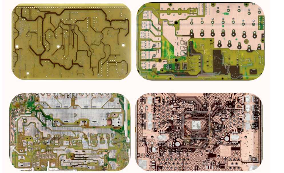
You start the process by drawing the PCBs that you want to develop later. If your drawing is not good, you can capture the PCBs and even scan them as alternative options. The purpose is to have a reference at the beginning of the process to make it easier for the overall development. If you are capturing the PCBs, then use a black background so that you can get clear and sharp pictures. You also need to take care of the light and use a good camera because you don’t want to mess up the pictures.
Bad quality and blurry pictures can totally ruin the designs, and reverse engineering results will be poor. Whatever you are going to choose, make sure to seek professional help if you are a beginner. Keep in mind that PCB reverse engineering is an extensive process and you don’t want to start everything from scratch if any of these steps does not take place properly. The next step is the uploading of images.
2. Uploading the Image
After you have clicked pictures of PCBs or have drawn the images now, you will upload them on the reverse engineering software that you are using. You can find tons of software for this purpose, depending on your needs. Cropping can be done if needed. Sometimes single software can help you with the entire design, but in some cases, you will have to switch between the software since their features are different. Again, it is a frustrating step, but the results will be worth it in the end. You just have to be well-adhered to your needs and choose the suitable software on that basis.
3. Constructing the Layout
It’s time to construct the layout of your PCBs. You need to use 3D visualization and 3D modeling for the development of these layouts. You can easily do this through your reverse engineering software since all of them have this option for creating layouts. Layouts, in this case, are important to showcase the distribution of electromagnetic fields and also provide insights into the performance of circuits to the users.
You can use schematics to have even more in-depth learning about PCB designs. The PCB layouts basically depend on the design and nature of PCBs. Complex PCBs need schematical layouts, which are the most intense.
We have compiled some crucial tips when it comes to PCB editing. Make sure to keep these tips in mind when you are done with your PCB layouts. Check them out below:
- Don’t forget to paint the holes and solder pads. By painting, we mean that you need to make upgrades in the pads and improve the efficiency of the holes. Also, make sure that these are tightly connected with the setup.
- There is no need to linger on the PCB trackpads, and you can use AutoTrace software to exclude them. These are redundant and eventually complicate your PCBs.
- Make sure to label the free holes. Free holes neither connect with anything nor join components. These are useless, and you have to label them as well.
- Work on the saturation and layers you have added by adjusting them as per your PCB designs.
- Untidy PCB tracks will not only confuse you but will also complicate your designs. You need to make sure that these are clean.
- Use grayscale on your design by removing the saturation. This process is the desaturation of the PCB images. You will use a white background after this. Combine it with software like AutoTrace to get positive results.
- You can simply repeat the same steps on the second side of PCBs because working on the double sides of PCBs is more suitable for the fine engineering of a PCB that meets industrial standards.
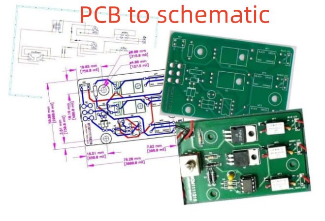
4. Creating Schematics
You can end this process with the development of PCB schematics. A schematic diagram is important to visualize and identify all the individual components of PCBs. This last step in reverse engineering basically prepares you for the practical development of PCBs.
Experts believes CAD is good software for the development of schematics. You can rely on the 2D version of CAD to make it all feasible for you. After this, you will combine it with AutoTrace to make sure everything is in place so that you can make the final changes if needed. When you combine such PCB development software, you ensure precision and design quality. It is important to consider for the producers because, in the end, this thing will lead to flawless and highly integrated PCBs.
When you’re done with the schematics, you will merge the sides of PCBs that you had developed earlier. You also need to name the components so that you can create an exact replica of the PCB design practically. There are different troubleshooting methods available that can save you time in case you need to rework some PCB parts. After making sure your PCB design is ready to interpret, you can begin with the final PCB production.
Drawbacks of reverse engineering a PCB
It is better to take a look at the negative side of PCB reverse engineering. So that you can look for alternatives. In fact, this is important so that you can evaluate your options without any struggle.
- The tracking of component connections is difficult in most cases.
- The important equipment used for reverse engineering might be inaccessible.
- The software used for this process can be highly expensive for some budding producers.
- The process demands high precision; therefore, the margin of error is next to impossible.
Conclusion
PCB reverse engineering is important to ensure PCB designs are in place and empower the producers to start production with no worries. Reverse engineering also rules out defects, faults, and technical issues since the process involves different steps in this regard. For the fine interpretation of PCB designs, you can never ignore PCB reverse engineering.
Different producers will find PCB reverse engineering expensive due to the high-end PCB design tools, but experts consider it crucial for the practical development of industrial-grade PCBs. We have provided all the insightful information regarding this process so that you won’t be struggling with PCB reverse engineering from now on.